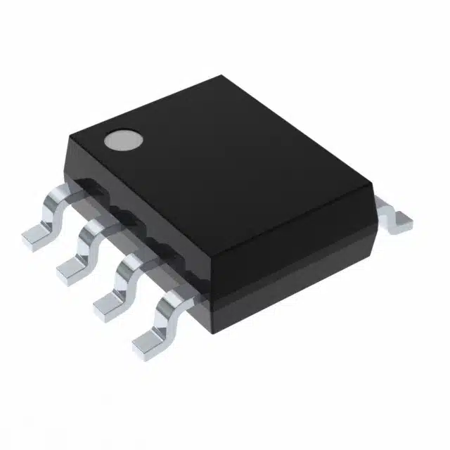
The 24lc512t-i/sm plays a vital role in communication systems by providing reliable non-volatile memory. It ensures data retention even during power loss. Its compatibility with the i2c protocol simplifies integration into embedded systems. Engineers use it for storing configuration settings, logging operational data, and retaining temporary information in various applications.
Key Takeaways
-
The 24LC512T-I/SM has 512 kilobits of memory that keeps data safe even if power goes out.
-
It uses the I2C protocol and can connect up to eight devices on one bus, making it easy to expand systems.
-
Setting up the A0, A1, and A2 pins correctly is important to avoid address problems and ensure smooth communication.
Key Features of the 24LC512 EEPROM IC
Memory Capacity and Organization
The 24LC512 EEPROM IC offers a memory capacity of 512 kilobits, organized as 64K x 8. This structure ensures efficient data storage and retrieval, making it suitable for applications requiring reliable non-volatile memory. The IC adheres to industry standards, ensuring compatibility with various embedded systems. Its adaptability allows engineers to use it in diverse scenarios, from storing configuration settings to logging operational data.
|
Memory Size |
Memory Organization |
Memory Interface |
|---|---|---|
|
512Kbit |
64K x 8 |
I²C |
I2C Communication Protocol and Multi-Device Support
The 24LC512 EEPROM IC uses the I2C communication protocol, which simplifies connectivity with microcontrollers. This protocol supports up to eight devices on the same bus, making it ideal for scalable systems. Chip select pins (A0, A1, A2) enable addressing multiple EEPROM units, while grounding these pins simplifies identification in single-device setups. This design ensures modularity and flexibility in communication systems.
|
Specification |
Details |
|---|---|
|
Communication Protocol |
I2C |
|
Device Cascading |
Supports up to 8 devices |
Operating Voltage Range and Power Efficiency
The 24LC512 EEPROM IC operates within a voltage range of 2.5V to 5.5V. This wide range ensures compatibility with various power supply configurations. Its low-power consumption enhances energy efficiency, making it an excellent choice for battery-powered communication systems. This feature reduces operational costs and extends the lifespan of devices.
|
Specification |
Value |
|---|---|
|
Operating Voltage Range |
2.5V to 5.5V |
|
Power Efficiency Contribution |
Low-power consumption |
Write Cycle Durability and Data Retention
The 24LC512 EEPROM IC provides exceptional write cycle durability, supporting up to 1 million write/erase cycles. This durability ensures long-term reliability, even in applications requiring frequent data updates. Additionally, the IC retains data for over 100 years, making it a dependable solution for storing critical information. The write protect pin further enhances data security by preventing accidental overwrites, ensuring data integrity in communication systems.
Tip: Always refer to the data sheet for detailed specifications and best practices when using the 24LC512 EEPROM IC.
Setting Up the 24LC512T-I/SM
Hardware Connections and Pin Configuration
Proper hardware connections ensure the 24LC512T-I/SM operates efficiently. The IC features eight pins, each serving a specific purpose. The table below outlines the pin configuration:
|
Pin Number |
Pin Name |
Description |
|---|---|---|
|
1, 2, 3 |
A0, A1, A2 |
User-configured Chip Select pins, useful during cascading |
|
4 |
Vss (Ground) |
Connected to the ground of the circuit |
|
5 |
Serial Data (SDA) |
Serial Data pin for I2C Communication |
|
6 |
Serial Clock (SCL) |
Serial Clock pin for I2C Communication |
|
7 |
Write-Protect |
If connected to Vss, write is enabled; if connected to Vcc, write is disabled |
|
8 |
Vcc |
Connect to supply rail |
To begin, connect the Vcc pin to the power supply and the Vss pin to the ground. Attach the SDA and SCL pins to the corresponding I2C communication lines of the microcontroller. Configure the A0, A1, and A2 pins based on the desired I2C address. For write protection, link the Write-Protect pin to Vss or Vcc as needed.
Configuring the I2C Address
The 24LC512T-I/SM supports multiple devices on the same I2C bus. Engineers can configure the I2C address using the A0, A1, and A2 pins. Each pin represents a bit in the address, allowing up to eight unique combinations. For example, grounding all three pins sets the address to 0x50 in hexadecimal. Adjust these pins to avoid conflicts when using multiple EEPROMs in a single system.
Software Initialization and Driver Setup
Software initialization ensures seamless communication between the microcontroller and the 24LC512T-I/SM. Begin by referencing the data sheet to understand the I2C protocol requirements. Load the appropriate driver for the microcontroller to handle I2C communication. Initialize the I2C bus by specifying the clock frequency and the EEPROM’s address. Test the setup by performing a basic read or write operation to verify functionality.
Tip: Always double-check connections and configurations before powering the system to prevent errors.
Performing Read and Write Operations
Writing Data to the 24LC512 EEPROM IC
Writing data to the 24lc512 eeprom ic involves sending the desired memory address and data through the I2C communication protocol. The process begins with the master device initiating a Start condition, followed by transmitting the control byte. The control byte contains the device address and the write bit (R/W set to ‘0’). After the EEPROM acknowledges the control byte, the master sends the memory address where the data will be stored. Once the address is acknowledged, the master transmits the data byte. The EEPROM acknowledges each byte and completes the write operation after receiving a Stop condition. Allow sufficient time for the write cycle to complete before initiating another operation.
Tip: Use the write protect pin to prevent accidental overwrites during critical operations.
Reading Data from the 24LC512 EEPROM IC
Reading data from the 24lc512 eeprom ic requires precise steps to ensure accuracy. The process varies depending on the type of read operation.
-
For a current address read, the master sends the control byte with the R/W bit set to ‘1’. The EEPROM transmits data from the last accessed address.
-
For a random read operation, the master first sends the desired word address as part of a write operation (R/W set to ‘0’). Then, it issues a repeated-Start condition and sends the control byte with R/W set to ‘1’.
-
For sequential reads, the master acknowledges each byte received and continues reading until the final byte. The master generates a Stop condition instead of an acknowledgment to terminate the operation.
Acknowledging data during sequential reads ensures accuracy. The master must avoid acknowledging the final byte to signal the EEPROM to stop transmission.
Addressing Memory Locations and Managing Slave Addresses
The 24lc512 eeprom ic uses a 16-bit memory addressing scheme, allowing access to all 64KB of memory. The master device specifies the memory location by sending the high and low bytes of the address during write or random read operations. Managing slave addresses becomes essential when multiple EEPROMs share the same I2C bus. Configure the A0, A1, and A2 pins to assign unique addresses to each device, ensuring seamless communication without conflicts.
Using Page Write for Efficient Data Storage
The page write feature of the 24lc512t-i/sm enhances efficiency by allowing up to 128 bytes of data to be written in a single operation. The master begins by sending the control byte, followed by the starting memory address and the data bytes. The EEPROM automatically increments the address within the page boundary. Exceeding the page limit causes the address to wrap around to the beginning of the page. This feature reduces the overhead of multiple write cycles, making it ideal for applications requiring bulk data storage.
Note: Ensure the data does not cross page boundaries to avoid overwriting unintended memory locations.
Error Handling and Troubleshooting
Resolving Common Read/Write Issues
Read and write issues in the 24LC512 eeprom often arise from improper connections or timing mismatches. Engineers should verify that the SDA and SCL lines are correctly connected to the microcontroller. Pull-up resistors on these lines ensure stable communication. Incorrect I2C clock frequency settings can also disrupt operations. Setting the clock frequency within the recommended range avoids timing errors. Additionally, ensuring the write protect pin is configured correctly prevents accidental write failures. Testing the system with small data blocks helps identify and resolve issues early.
Address Conflict Resolution in Multi-Device Systems
Address conflicts occur when multiple eeprom devices share the same I2C address. Engineers can resolve these conflicts using several techniques:
-
Configure the A0, A1, and A2 pins to assign unique addresses to each device.
-
Use I/O lines on the microcontroller to force the SDA lines high for inactive devices while setting the targeted device’s I/O line as input.
-
Add resistors to the SDA line for inactive devices to act as pull-ups.
-
Employ Schottky diodes to allow devices to pull the SDA line low during data transmission.
-
Consider I2C bus multiplexers or switch ICs for managing multiple devices effectively.
These methods ensure seamless communication between the master and slave devices.
Verifying Data Integrity and Debugging Communication Failures
Data integrity is critical in communication systems. Engineers should verify data by reading back stored values and comparing them with the original data. Noise on the I2C bus can cause communication failures. Shielded cables and proper grounding reduce interference. Debugging tools, such as logic analyzers, help monitor the I2C signals and identify errors. Checking for acknowledgment signals from the eeprom ensures successful data transmission. Regular testing and monitoring maintain system reliability.
The 24lc512t-i/sm simplifies data storage in communication systems with its reliable features. Engineers should follow proper setup steps, including hardware connections and I2C address configuration. Addressing and error handling ensure smooth operation. Testing small data blocks verifies functionality. Pull-up resistors stabilize I2C communication, reducing errors. These practices enhance system reliability and performance.
What is the maximum number of devices that can share the same I2C bus?
The 24LC512T-I/SM supports up to eight devices on a single I2C bus. Engineers configure unique addresses using the A0, A1, and A2 pins.
How can engineers prevent accidental data overwrites?
The Write-Protect pin ensures data security. Connecting it to Vcc disables write operations, while linking it to Vss enables writing. This feature safeguards critical information.
What tools help debug I2C communication issues?
Logic analyzers monitor I2C signals and identify errors. Engineers use these tools to verify acknowledgment signals and ensure successful data transmission between devices.
See Also
Three Effective Methods for MC9S12XET512VAG Integration
Understanding MC9S12DJ256MFUE Specs for Automotive Use
Key Specifications of the MC9S12XEQ512CAL Unveiled
Fundamental Programming Techniques for MC9S12XD256 Controllers
Simple Guide to Integrating SN74LVC4245APW Sensors