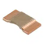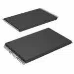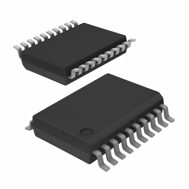
The 74FCT3807PYG8, also known by its part aliases IDT74FCT3807PYG8 and 74FCT3807, is a low-skew clock driver designed to provide precise timing and synchronization in advanced systems. Its innovative design ensures accurate signal distribution, which is vital for maintaining reliable communication in telecommunications. Featuring a fanout capability of 1:10 and compatibility with both 3.3V and 5V components, it enables seamless integration into a variety of architectures. This clock driver is essential in high-speed digital circuits, where timing accuracy and signal integrity are critical for achieving optimal performance.
Key Takeaways
-
The 74FCT3807PYG8 is essential for precise timing and synchronization in telecommunications, ensuring reliable communication across systems.
-
With a fanout capability of 1:10, this clock driver can efficiently distribute a single clock signal to multiple outputs, enhancing system performance.
-
Its compatibility with both 3.3V and 5V components allows for seamless integration into various architectures, making it versatile for engineers.
-
The low-skew design minimizes timing discrepancies, which is critical for maintaining synchronization in high-speed digital circuits.
-
Advanced dual metal CMOS technology reduces power consumption and noise, ensuring stable operation even in demanding environments.
-
The 74FCT3807PYG8 is poised to support next-generation telecom systems, including 5G and IoT, by delivering the timing accuracy required for these advanced applications.
-
Engineers should conduct thorough system analysis and testing to ensure successful integration of the 74FCT3807PYG8 into existing telecom infrastructures.
What is the 74FCT3807PYG8 Clock Driver?
Definition and Purpose
The 74FCT3807PYG8 is a high-performance clock driver designed to meet the demands of modern telecommunications and digital systems. It ensures precise timing and synchronization, which are critical for maintaining the integrity of high-speed signals. This device features a fanout capability of 1:10, allowing it to distribute a single input clock signal to up to ten outputs with minimal skew. Its compatibility with both 3.3V and 5V components makes it versatile for integration into various system architectures.
Engineered using advanced dual metal CMOS technology, the 74FCT3807PYG8 delivers low power consumption and reduced noise levels. These characteristics make it an ideal choice for applications requiring reliable clock distribution and signal integrity. By improving timing accuracy, this clock driver supports the seamless operation of processors, network equipment, and other high-speed digital circuits.
Overview of its Role in Signal Timing and Synchronization
In telecommunications, timing and synchronization are essential for ensuring smooth communication between devices. The 74FCT3807PYG8 plays a pivotal role in achieving this by distributing clock signals with low skew. Low skew minimizes timing discrepancies between signals, which is crucial for maintaining synchronization across interconnected systems.
This clock driver also enhances signal integrity by reducing noise and jitter, which can disrupt data transmission. Its ability to operate efficiently in high-speed environments makes it indispensable for applications such as base stations, data centers, and networking equipment. By providing accurate timing, the 74FCT3807PYG8 supports the reliable performance of systems that depend on precise signal coordination.
“Timing is everything in telecommunications. The 74FCT3807PYG8 ensures that every signal arrives exactly when it should, enabling flawless communication.”
Technical Specifications of the 74FCT3807PYG8
Key Features
The 74FCT3807PYG8 offers a range of features that make it a standout choice for clock distribution in telecommunications and high-speed digital systems. Its low-skew design ensures precise timing, which is essential for maintaining synchronization across interconnected devices. The fanout capability of 1:10 allows a single input clock signal to drive up to ten outputs, providing efficient signal distribution without compromising accuracy.
This clock driver supports both 3.3V and 5V input levels, enhancing its versatility for integration into various system architectures. Advanced dual metal CMOS technology reduces power consumption and minimizes noise, ensuring reliable performance even in demanding environments. Additionally, the device incorporates low input capacitance with hysteresis, which improves noise margins and enhances signal integrity.
Performance Metrics
The performance of the 74FCT3807PYG8 reflects its high-quality engineering. It delivers low propagation delay, which ensures that signals are transmitted quickly and accurately. The low skew between output signals, typically measured in picoseconds, guarantees minimal timing discrepancies. This precision is critical for applications requiring high-speed data processing and communication.
The device also exhibits excellent noise reduction capabilities. By minimizing power and ground noise, it maintains signal clarity and reduces the risk of data errors. Its robust design ensures consistent performance across a wide temperature range, making it suitable for use in diverse operating conditions.
Compatibility with System Architectures
The 74FCT3807PYG8 demonstrates exceptional compatibility with modern system architectures. Its ability to operate with both 3.3V and 5V components simplifies integration into existing designs. This flexibility allows engineers to use the device in a variety of applications, from legacy systems to cutting-edge technologies.
The clock driver supports seamless operation in systems that require precise timing and synchronization. Its design aligns with the needs of processors, network equipment, and other high-speed digital circuits. By offering compatibility with multiple output types, such as LVPECL, LVDS, and HSTL, it adapts to the specific requirements of different telecommunications and data center infrastructures.
How the 74FCT3807PYG8 Functions
Operating Principles
The 74FCT3807PYG8 operates as a low-skew clock driver, ensuring precise timing and synchronization in high-speed systems. It takes an input clock signal and distributes it to multiple outputs with minimal delay. This process relies on its advanced dual metal CMOS technology, which enhances signal integrity and reduces power consumption. The device’s fanout capability of 1:10 allows it to drive up to ten outputs from a single input, maintaining consistent timing across all channels.
The clock driver minimizes skew, which refers to the difference in arrival times of signals at different outputs. By keeping skew levels low, it ensures that all connected components receive signals simultaneously. This synchronization is critical for systems that require coordinated operations, such as telecommunications networks and data centers. The device also incorporates low input capacitance with hysteresis, which improves noise margins and ensures stable signal transmission.
Role in Signal Distribution and Noise Reduction
The 74FCT3807PYG8 plays a vital role in distributing clock signals efficiently while maintaining signal quality. Its design ensures that the output signals remain consistent and free from distortion. This consistency is essential for high-speed digital circuits, where even minor timing errors can disrupt system performance. The device’s ability to handle both 3.3V and 5V input levels adds flexibility, making it suitable for various system architectures.
Noise reduction is another key function of this clock driver. The 74FCT3807PYG8 minimizes power and ground noise, which can interfere with signal clarity. By reducing noise, it enhances the reliability of data transmission and prevents errors. Its low-skew performance further contributes to noise reduction by ensuring that signals arrive at their destinations without unnecessary delays or variations.
In telecommunications, the device supports seamless communication by maintaining synchronization across interconnected systems. It ensures that signals are distributed accurately, enabling smooth operation of base stations, network equipment, and other critical infrastructure. Its robust design and reliable performance make it an indispensable component in modern telecom systems.
Applications of the 74FCT3807PYG8 in Telecommunications
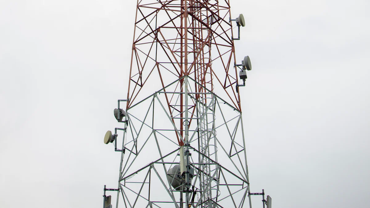
Use in Base Stations and Network Infrastructure
The 74FCT3807PYG8 plays a crucial role in base stations and network infrastructure. Base stations rely on precise timing to manage communication between devices and ensure seamless data transmission. This clock driver distributes clock signals with low skew, enabling synchronized operations across multiple components. By maintaining accurate timing, it supports the efficient handling of high volumes of data traffic.
Network infrastructure also benefits from the device’s ability to reduce noise and jitter. These features enhance signal integrity, which is essential for reliable communication. The 74FCT3807PYG8 ensures that signals remain clear and consistent, even in demanding environments. Its compatibility with both 3.3V and 5V systems allows engineers to integrate it into various network designs, from legacy systems to modern architectures.
Role in Data Centers and High-Speed Digital Circuits
Data centers depend on high-speed digital circuits to process and transmit vast amounts of information. The 74FCT3807PYG8 ensures precise timing in these circuits, which is critical for maintaining system performance. Its low-skew design minimizes timing discrepancies, allowing data to flow smoothly between interconnected components.
In high-speed environments, noise can disrupt operations and lead to errors. The 74FCT3807PYG8 addresses this challenge by reducing power and ground noise, ensuring stable signal transmission. Its advanced technology supports the synchronization of processors and other critical hardware, enabling efficient data processing.
The device’s versatility extends to its use in various high-speed applications. Engineers can implement it in systems requiring precise timing, such as cloud computing platforms and advanced networking equipment. Its robust performance and reliability make it an indispensable component in modern data centers.
Advantages of Using the 74FCT3807PYG8
Reliability and Precision in Timing
The 74FCT3807PYG8 ensures exceptional reliability in timing, which is critical for high-speed digital systems. Its low-skew design minimizes timing discrepancies, allowing signals to arrive at their destinations with precision. This accuracy supports seamless synchronization across interconnected components, ensuring smooth operations in telecommunications and data processing environments. The device’s ability to maintain consistent performance under varying conditions further enhances its reliability, making it a trusted choice for engineers.
Precision in timing plays a vital role in preventing errors and maintaining data integrity. The 74FCT3807PYG8 achieves this by reducing jitter and noise, which can disrupt signal clarity. By delivering stable and accurate clock signals, it supports the efficient functioning of processors, network equipment, and other critical hardware. Its robust design ensures that timing remains consistent even in demanding applications, such as base stations and data centers.
Efficiency and Flexibility in Integration
The 74FCT3807PYG8 offers remarkable efficiency in clock signal distribution. Its fanout capability of 1:10 allows a single input to drive multiple outputs without compromising signal quality. This feature reduces the need for additional components, simplifying system design and lowering overall costs. The device’s low power consumption further contributes to its efficiency, making it suitable for energy-conscious applications.
Flexibility in integration is another key advantage of the 74FCT3807PYG8. Its compatibility with both 3.3V and 5V components enables seamless incorporation into various system architectures. Engineers can use it in legacy systems or modern designs without extensive modifications. Additionally, its support for multiple output types, such as LVPECL and LVDS, ensures adaptability to diverse requirements. This versatility makes it an ideal solution for a wide range of telecommunications and high-speed digital applications.
Comparison to Other Clock Drivers
The 74FCT3807PYG8 stands out when compared to other clock drivers due to its combination of performance, reliability, and versatility. Many clock drivers lack the low-skew capabilities that this device provides, which are essential for maintaining precise timing. Its advanced dual metal CMOS technology also sets it apart by reducing noise and power consumption, ensuring stable operation in high-speed environments.
While some clock drivers may offer similar fanout capabilities, the 74FCT3807PYG8 excels in its ability to maintain signal integrity across all outputs. Its compatibility with both 3.3V and 5V systems adds another layer of flexibility that many alternatives cannot match. These features make it a superior choice for applications requiring precise timing, efficient signal distribution, and reliable performance.
“The 74FCT3807PYG8 redefines clock driver performance by combining precision, efficiency, and adaptability, making it a standout solution for modern telecommunications.”
Challenges and Considerations for the 74FCT3807PYG8
Integration with Existing Telecom Systems
Integrating the 74FCT3807PYG8 into existing telecom systems requires careful planning and execution. Engineers must evaluate the compatibility of the clock driver with the current system architecture. This evaluation includes assessing voltage levels, signal types, and timing requirements. The device supports both 3.3V and 5V components, which simplifies integration in many cases. However, ensuring seamless operation still demands a thorough understanding of the system’s design.
Telecom systems often involve legacy infrastructure alongside modern components. The 74FCT3807PYG8 must bridge this gap effectively. Engineers need to verify that the clock driver aligns with the timing protocols and synchronization standards of the existing setup. Any discrepancies in timing or signal distribution could disrupt communication and affect overall performance. Testing and validation play a critical role in ensuring smooth integration.
“Successful integration of the 74FCT3807PYG8 depends on meticulous planning and a deep understanding of system requirements.”
Addressing Design and Application Constraints
Design constraints can pose challenges when implementing the 74FCT3807PYG8 in telecom systems. Engineers must consider factors such as space limitations, power consumption, and thermal management. The compact design of the clock driver helps address space concerns, making it suitable for densely packed systems. Its low power consumption also reduces the strain on energy resources, which is vital for efficient operation.
Application-specific requirements may introduce additional constraints. For instance, high-speed environments demand minimal skew and jitter to maintain signal integrity. The 74FCT3807PYG8 meets these requirements with its low-skew design and noise reduction capabilities. However, engineers must ensure that the device operates within its specified parameters to achieve optimal performance.
To address these challenges, engineers often follow a structured approach:
-
System Analysis: Identify the specific needs and constraints of the application.
-
Component Selection: Verify that the 74FCT3807PYG8 meets the technical requirements.
-
Prototyping and Testing: Validate the performance of the clock driver in real-world conditions.
-
Optimization: Fine-tune the design to overcome any identified limitations.
By following these steps, engineers can effectively address design and application constraints while leveraging the full potential of the 74FCT3807PYG8.
“Overcoming design constraints requires a balance between technical expertise and innovative problem-solving.”
Future Trends and Developments for the 74FCT3807PYG8
Innovations in Clock Driver Technology
The evolution of clock driver technology continues to address the growing demands of high-speed digital systems. Manufacturers like Renesas have introduced advanced dual metal CMOS technology, which enhances the performance of devices such as the 74FCT3807PYG8. This innovation reduces power consumption and improves noise margins, ensuring reliable operation in complex environments. The integration of low input capacitance and hysteresis further strengthens signal integrity, making these devices indispensable for modern telecommunications.
Emerging trends also highlight the development of phase-locked loop (PLL)-based clock drivers. These devices offer enhanced timing precision by synchronizing output signals with a reference clock. Such advancements pave the way for even lower skew and jitter, which are critical for maintaining synchronization in high-speed networks. Additionally, hardware-specific clock driver functions are being tailored to meet the unique requirements of various systems, providing optimized solutions for diverse applications.
The collaboration between industry leaders, such as Intel and Renesas, has accelerated the pace of innovation. Their joint efforts focus on creating next-generation clock drivers that cater to the needs of evolving markets. These advancements aim to deliver higher speeds, improved reliability, and greater flexibility, ensuring that devices like the 74FCT3807PYG8 remain at the forefront of clock distribution technology.
“The future of clock driver technology lies in precision, efficiency, and adaptability, driven by continuous innovation and collaboration.”
Role in Next-Generation Telecom Systems (e.g., 5G and IoT)
The 74FCT3807PYG8 is poised to play a significant role in next-generation telecom systems, including 5G networks and the Internet of Things (IoT). These systems demand unparalleled timing accuracy and synchronization to support their high-speed and low-latency requirements. The low-skew design of the 74FCT3807PYG8 ensures precise signal distribution, making it an ideal choice for these advanced applications.
In 5G networks, the need for efficient clock distribution becomes even more critical. Base stations and network infrastructure must handle massive data volumes while maintaining synchronization across multiple components. The 74FCT3807PYG8 addresses these challenges by delivering consistent performance and reducing noise, ensuring seamless communication between devices.
IoT ecosystems also benefit from the capabilities of this clock driver. IoT devices rely on accurate timing to coordinate operations and transmit data efficiently. The versatility of the 74FCT3807PYG8, with its compatibility across different voltage levels and output types, makes it suitable for a wide range of IoT applications. Its robust design ensures reliable performance in diverse environments, from smart cities to industrial automation.
As telecom systems continue to evolve, the 74FCT3807PYG8 will remain a cornerstone of clock distribution technology. Its ability to adapt to the demands of next-generation networks ensures its relevance in shaping the future of telecommunications.
“The 74FCT3807PYG8 bridges the gap between current technologies and the future of telecommunications, supporting the seamless operation of 5G and IoT systems.”
The 74FCT3807PYG8 stands out as a vital component in modern telecommunications. Its low-skew design, high fanout capability, and compatibility with diverse system architectures ensure precise timing and synchronization. These features make it indispensable for maintaining reliable communication across telecom systems. By enhancing efficiency and signal integrity, it supports robust and efficient telecommunications infrastructure. Its adaptability to next-generation technologies, such as 5G and IoT, highlights its potential to drive future advancements. This clock driver remains a cornerstone for engineers seeking precision and reliability in high-speed digital systems.
See Also
Enhancing Process Control With AD74413RBCPZ Unlocking
Transform Your Projects Using EP2C50F484I8N FPGA
Simple Networking Tips for XILINX XC7K325T-2FFG676C
Understanding MC9S12DJ256MFUE Specs for Automotive Use
Three Effective Methods to Integrate MC9S12XET512VAG