Reliable data transfer is crucial in digital systems. This is especially true when you interface with memory buffers. Without proper synchronization, you face common challenges. These include timing mismatches, race conditions, and data corruption. For example, 67% of ERP failures come from process design flaws, with synchronization mismatches being the largest subcategory. Moreover, concurrent access to shared buffers often corrupts data. This happens when a processor’s cache and main memory do not align. The 74HC74D Integrated Circuits offer a fundamental and effective solution. You can use the 74HC74D FOR Memory Buffers to solve these issues. This component, the 74HC74D FOR Memory Buffers, sets the stage for a deep dive into its applications.
Key Takeaways
-
The 74HC74D chip helps fix common problems in digital systems. It stops data from getting corrupted. It also prevents timing issues when data moves to memory.
-
This chip works like a gatekeeper for data. It only lets data pass when a clock signal tells it to. This makes sure data arrives at the memory at the right time.
-
The 74HC74D prevents data errors. It makes sure data is stable before the memory uses it. This keeps your system reliable and accurate.
-
You can connect the 74HC74D between your data source and memory. This makes sure the data is perfectly timed for the memory. You can also use its special pins to reset or set the data.
-
For wider data paths, you can use several 74HC74D chips together. This lets you synchronize many data lines at once. This keeps all your data moving correctly.
Memory Buffer Synchronization Challenges
When you work with memory buffers, you face several critical challenges. These issues can compromise data integrity and system performance. You must understand these problems to design robust solutions.
The Need for Data Alignment
You need proper data alignment for efficient memory operations. High-speed memory buffers, like those in DirectX11, often require 16-byte alignment. This alignment helps with faster memory copying operations. For example, memcpy() benefits from aligned SSE store/load operations. Aligned data also fits better within a single CPU cache line. This avoids performance penalties from reading multiple cache lines for unaligned data. Modern CPU features, such as SIMD instructions, often have strict alignment requirements. Unaligned data can slow down your system or even cause it to fail. In C++, you can use the alignas specifier. This explicitly requests specific memory alignment for your variables. It ensures optimal performance and prevents awkward cache line crossings.
Common Timing Violations
You will encounter frequent timing violations in memory buffer designs. Increased insertion delay can lead to setup time violations. It can also cause hold time violations or clock skew issues. Signal propagation time increases, potentially failing to meet design constraints. Decreased insertion delay might seem good. However, it can introduce new timing violations. Faster signal transitions might violate timing requirements. Setup violations happen when data arrives too late. This is common with higher clock frequencies and tighter timing windows. Hold violations occur when data becomes unstable too soon after the clock edge. Clock skew, early data arrival, and short paths often cause these. This is especially true in ultra-fast designs with tight pipelining.
Consequences of Asynchronous Data
Asynchronous data can lead to serious problems. You might experience data corruption. This means your stored information becomes incorrect. Your system could also suffer from race conditions. Different parts of your system try to access the same data at the same time. This leads to unpredictable results. Ultimately, your system’s reliability decreases. You also see a drop in overall performance. These issues make your digital system unstable and inefficient.
74HC74D: Dual D-Type Flip-Flop Fundamentals
The 74HC74D is a high-speed CMOS dual D-type flip-flop. This component responds to a positive clock edge. It offers two independent flip-flops within one package. You can use it for many tasks beyond just synchronization. For example, it stores data, builds registers, and creates counters. This versatility makes it a fundamental building block in digital design.
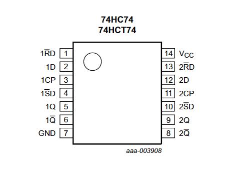
Pin Configuration and Functions
You will find specific pins on the 74HC74D, each with a clear function. Understanding these pins helps you connect the device correctly.
-
D (Data Input): You apply the data you want to store here.
-
CLK (Clock Input): This pin controls when the flip-flop captures data.
-
nSD (Preset/Set Input): This active-low input forces the Q output high, overriding other inputs.
-
nRD (Clear/Reset Input): This active-low input forces the Q output low, overriding other inputs.
-
Q (Output): This pin provides the stored data.
-
Q-bar (Complementary Output): This pin provides the inverse of the stored data.
-
VCC (Supply Voltage): You connect the positive power supply here.
-
GND (Ground): You connect the ground reference here.
Edge-Triggered Operation Explained
The 74HC74D operates based on the clock signal’s edge. It is a positive-edge-triggered device. This means the flip-flop only captures the data present at its D input when the clock signal transitions from a low voltage to a high voltage. At all other times, the output (Q) remains unchanged. This precise timing control is crucial for synchronization. You ensure data transfers only at specific, controlled moments. This prevents unwanted changes and maintains data integrity. The flip-flop ignores any changes on the D input when the clock is stable or transitioning downwards.
74HC74D for Memory Buffers: Core Synchronization
You use the 74HC74D to create a robust bridge between your data source and memory. This component acts as a crucial synchronizer. It ensures data arrives at the memory buffer precisely when needed. This prevents many common timing problems. The 74HC74D FOR Memory Buffers provides a reliable mechanism for data integrity. You achieve stable and predictable system operation.
How 74HC74D Achieves Data Alignment
The 74HC74D plays a vital role in aligning your data. It acts as a temporary storage unit. You feed your asynchronous data into its D input. The memory’s write clock connects to the 74HC74D’s clock input. The flip-flop then samples the data only on the rising edge of this clock. This means the output (Q) changes state only at a specific, controlled moment.
Tip: Think of the 74HC74D as a gatekeeper. It opens its gate to let data through only when the clock signal gives the exact command. This ensures the data is perfectly timed for the memory.
This edge-triggered behavior ensures your data aligns perfectly with the memory’s internal timing. The memory expects data to be stable at certain points in its clock cycle. The 74HC74D delivers this stability. You eliminate the guesswork of when data will arrive. This creates a predictable data stream for your memory buffer.
Mitigating Setup and Hold Time Issues
You can effectively mitigate setup and hold time issues with the 74HC74D. Memory devices have strict timing requirements. They need data to be stable for a certain period before the clock edge (setup time). They also need data to remain stable for a period after the clock edge (hold time). If these conditions are not met, the memory might read incorrect data.
The 74HC74D isolates the memory from the raw, potentially unstable data source. When the 74HC74D captures data on a clock edge, its Q output becomes stable. This stable output then feeds directly into your memory’s data input. The flip-flop holds this data steady for the entire clock cycle until the next rising edge. This provides ample time for the memory to meet its setup and hold time requirements. You ensure the memory always sees valid, stable data during its critical sampling window. This makes your system much more reliable.
Preventing Data Corruption
You prevent data corruption by using the 74HC74D. Unsynchronized data can lead to race conditions. This happens when the memory tries to read or write data while the data itself is still changing. This results in the memory capturing an undefined or incorrect value. The 74HC74D FOR Memory Buffers eliminates this risk.
By synchronizing the data to the memory’s clock, you ensure data stability. The flip-flop’s output provides a clean, stable signal. This signal is ready for the memory at the precise moment of its clock edge. You avoid situations where the memory samples data during a transition. This guarantees that the data written to or read from the memory buffer is always the intended value. You maintain the integrity of your stored information. This leads to a more robust and error-free digital system.
74HC74D in Memory Buffers: Practical Implementation
You now understand the theoretical benefits of the 74HC74D. Let’s explore how you practically implement this component in your memory buffer designs. Proper connection and utilization of its control inputs are key to successful synchronization.
Connecting Data and Clock Inputs
Connecting the 74HC74D correctly is straightforward. You place it directly in the data path between your asynchronous data source and your synchronous memory buffer.
-
Data Source to D Input: You connect the output of your asynchronous data source directly to the D (Data) input of the 74HC74D. This is the data you want to synchronize.
-
Memory Write Clock to CLK Input: You connect the memory’s write clock signal to the CLK (Clock) input of the 74HC74D. This clock dictates when the flip-flop captures the data. The 74HC74D samples the data on the rising edge of this clock.
-
74HC74D Output to Memory Input: You connect the Q output of the 74HC74D to the data input pin of your memory buffer. The stable, synchronized data from the flip-flop then feeds directly into the memory.
This setup ensures that the data presented to the memory is always stable and aligned with the memory’s own clock cycle. You effectively isolate the memory from any timing uncertainties of the original data source.
Using Preset and Clear for Control
The 74HC74D also provides powerful control inputs: preset (nSD) and clear (nRD). These inputs are active-low, meaning they perform their function when you apply a logic LOW (0V) signal.
-
Preset (nSD): When you pull the nSD input LOW, it immediately forces the Q output HIGH, regardless of the clock or D input. You use this for initial state setting. For example, you can set a memory buffer to an all-ones state at system startup.
-
Clear (nRD): When you pull the nRD input LOW, it immediately forces the Q output LOW, overriding all other inputs. You use this for resetting the flip-flop. This is useful for clearing a memory buffer or for error recovery scenarios, bringing the system to a known, safe state.
You typically keep both nSD and nRD HIGH during normal operation. This allows the flip-flop to respond to the D and CLK inputs. You only activate them when you need to force a specific output state. This precise control enhances the reliability of your system, especially when using the 74HC74D FOR Memory Buffers.
Example Circuit Configurations
Imagine you have a sensor providing data asynchronously. You want to write this data into a synchronous RAM buffer. Here is a conceptual setup:
+-----------------+       +-----------------+       +-----------------+
| Asynchronous    |       |     74HC74D     |       | Synchronous     |
| Data Source     |------>| D Input         |------>| Data Input (RAM)|
| (Sensor Output) |       |                 |       |                 |
+-----------------+       | CLK Input       |       | Write Clock     |
                          | (Memory Write   |<------| (from Memory    |
                          |  Clock)         |       | Controller)     |
                          |                 |       |                 |
                          | nSD (Preset)    |<------| (System Reset/  |
                          | nRD (Clear)     |<------|  Control Logic) |
                          +-----------------+       +-----------------+
In this configuration, the 74HC74D acts as a crucial intermediary. It captures the sensor data only when the memory controller issues a write clock pulse. This ensures the RAM receives data that is perfectly aligned with its internal timing requirements. You can also use the nSD and nRD inputs to initialize the RAM’s input register or clear it if an error occurs. This makes the 74HC74D FOR Memory Buffers an indispensable tool for robust data handling. You gain significant control over data flow and integrity.
Advanced 74HC74D Use and Best Practices
You can optimize your designs further with the 74HC74D. Understanding advanced concepts helps you build more robust systems. You ensure maximum reliability and performance.
Managing Clock Skew and Signal Integrity
Clock skew occurs when the clock signal arrives at different components at slightly different times. This can cause timing violations. You must manage clock skew carefully. Use short, direct clock traces. You can also employ clock buffers to distribute the clock signal evenly. Good signal integrity is also vital. You prevent noise and reflections on your signal lines. Use proper termination resistors on high-speed signals. You also route data lines away from noisy power traces. This ensures your 74HC74D receives clean, stable inputs.
Propagation Delay Considerations
Every digital component introduces a slight delay. This is propagation delay. The 74HC74D has its own propagation delay. This is the time it takes for an input change to reflect at the output. You must account for this delay in your timing calculations. For example, if your memory requires data within 10ns, and the 74HC74D has a 5ns delay, you only have 5ns left for other delays. Always check the datasheet for specific propagation delay values. You ensure your overall system timing meets all requirements.
Cascading for Wider Data Buses
The 74HC74D contains two independent flip-flops. This handles two bits of data. Many memory buffers use wider data buses, like 8-bit or 16-bit. You can cascade multiple 74HC74D chips to synchronize these wider buses. For an 8-bit bus, you would use four 74HC74D chips. Each chip synchronizes two data lines. You connect the same clock signal to all CLK inputs. You also connect the same preset and clear signals to all nSD and nRD inputs. This ensures all data bits synchronize simultaneously. You maintain data integrity across the entire bus.
You now see the 74HC74D’s vital role. It ensures robust data synchronization in memory buffers. Its precise edge-triggered behavior effectively solves common timing problems. You mitigate setup and hold issues. This guarantees data integrity. Apply these principles. You will design more reliable and stable digital systems. This foundational knowledge empowers you.
FAQ
What is the main purpose of the 74HC74D in memory buffers?
You use the 74HC74D to synchronize data. It ensures data arrives at the memory buffer at the correct time. This prevents timing mismatches and data corruption.
Why is data synchronization critical for memory buffers?
Data synchronization prevents issues like race conditions and data corruption. It ensures your memory receives stable, correct data. This makes your digital system reliable and efficient.
How do you use the Preset and Clear inputs on the 74HC74D?
You use Preset (nSD) to force the output high. You use Clear (nRD) to force the output low. These active-low inputs help you set initial states or recover from errors.
Can you use the 74HC74D for wider data buses?
Yes, you can. You cascade multiple 74HC74D chips. Each chip handles two data bits. You connect the same clock and control signals to all chips. This synchronizes the entire bus.
See Also
Mastering MC9S12XD256 Microcontrollers: Essential Programming Techniques and Applications
MC9S12DJ256MFUE: Automotive Electronics’ Core Component, Explored and Implemented Practically
MC9S12XET512VAG Microcontroller: Automotive System Integration Strategies and Practical Analysis
AD9736BBCZ: Shaping the Future of Advanced Wireless Communication Technologies
MC9S12XEQ512CAL: Deep Dive into Automotive and Industrial Control Applications