The LT1801IMS8 offers exceptional performance for noise-free sensor signal amplification. Its low input offset voltage of 75 μV and high slew rate of 25 V/μs ensure precise and rapid signal processing. Engineers value its ability to amplify signals with minimal distortion, even in challenging environments. The LT1801IMS8#PBF also features a gain bandwidth product of 80 MHz, making it ideal for high-speed applications. The following table highlights its key specifications:
|
Feature |
LT1801IMS8 |
|---|---|
|
Input Offset Voltage |
75 μV |
|
Input Bias Current |
25 nA |
|
Gain Bandwidth Product (GBP) |
80 MHz |
|
Slew Rate |
25 V/μs |
|
Power Supply Rejection Ratio |
98 dB |
|
Common Mode Rejection Ratio |
105 dB |
|
Output Current per Channel |
45 mA |
These attributes make the LT1801IMS8 a reliable choice for precision applications requiring clean and accurate signal amplification.
Key Takeaways
-
The LT1801IMS8 amplifier is fast and quiet, perfect for clear signal boosting.
-
It has an 80 MHz bandwidth and a 25 V/μs speed, allowing quick and precise signal handling in fast systems.
-
Engineers can adjust gain by picking the right resistors, ensuring good signal boosting for different sensors.
-
A good PCB design is important; keeping wires short and grounding well improves performance and cuts noise.
-
The LT1801IMS8 works with many sensors, making it useful for both factories and everyday gadgets.
Overview of LT1801IMS8
Key Features of LT1801IMS8
Low noise and high-speed performance
The LT1801IMS8 delivers exceptional low-noise performance, making it ideal for applications requiring clean signal amplification. Its high slew rate of 25 V/μs ensures rapid response to input changes, which is critical for high-speed systems. The dual op-amp design further enhances its ability to process signals efficiently while maintaining low distortion. These features make it a preferred choice for engineers working on precision systems.
Wide bandwidth and low input offset voltage
With an impressive gain bandwidth of 80 MHz, the LT1801IMS8 supports fast and accurate signal processing. The low input offset voltage of 75 μV ensures precise amplification, minimizing errors in sensitive applications. This combination of wide bandwidth and low offset voltage allows the amplifier to handle complex signals with high fidelity.
|
Feature |
Specification |
|---|---|
|
Gain Bandwidth |
80 MHz |
|
Slew Rate |
25 V/μs |
|
Input Offset Voltage |
75 μV |
|
Input Bias Current |
25 nA |
|
Supply Voltage Range |
2.3V to 12.6V |
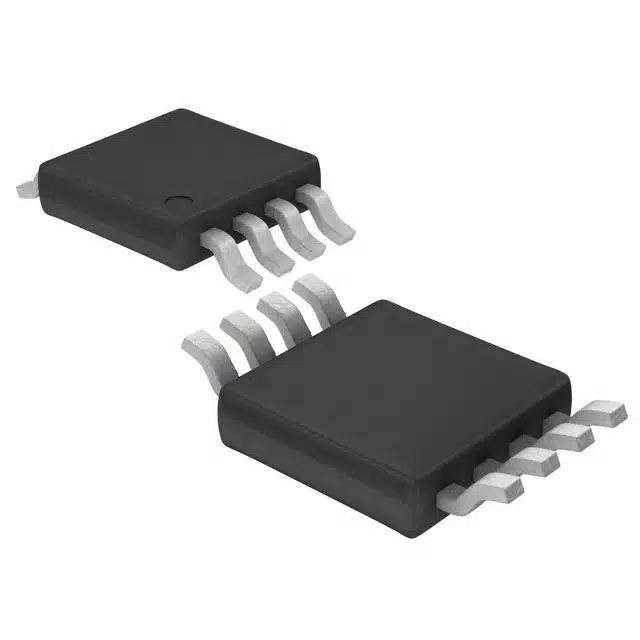
Compact MSOP-8 package for space-constrained designs
The LT1801IMS8 comes in a compact MSOP-8 package, making it suitable for designs where space is limited. This small form factor allows engineers to integrate it into portable devices, medical instruments, and other compact systems without compromising performance. Its rail-to-rail operation further enhances its versatility in various applications.
Benefits for Noise-Free Signal Amplification
High accuracy and precision in signal processing
The LT1801IMS8 ensures high accuracy in signal processing due to its low input offset voltage and bias current. These attributes reduce errors, enabling precise readings in applications like medical devices and instrumentation.
Effective noise reduction for clean signal output
The amplifier’s low noise characteristics and high common-mode rejection ratio (CMRR) effectively suppress unwanted noise. This ensures clean signal output, even in environments with significant electrical interference.
|
Feature |
Value |
|---|---|
|
Input Offset Voltage |
75 μV |
|
Input Bias Current |
25 nA |
|
Gain Bandwidth Product |
80 MHz |
|
Slew Rate |
25 V/μs |
Compatibility with various sensor types
The LT1801IMS8 supports a wide range of sensors, including thermocouples, strain gauges, and photodiodes. Its wide supply voltage range (2.3V to 12.6V) and low power consumption make it adaptable to diverse applications. Engineers can rely on its performance for both industrial and consumer-grade systems.
LT1801IMS8 in Sensor Interfaces
Noise Reduction in Sensor Signals
Differential input design for rejecting common-mode noise
The LT1801IMS8 excels in rejecting common-mode noise through its differential input design. This feature allows the amplifier to process the difference between two input signals while ignoring noise that is common to both. This capability is particularly beneficial in environments with significant electrical interference, such as industrial settings or medical equipment. By rejecting unwanted noise, the LT1801IMS8 ensures that the amplified signal remains clean and accurate, which is essential for precision applications.
Low input bias current for minimal signal distortion
The LT1801IMS8 features a low input bias current of 25 nA, which plays a critical role in maintaining signal integrity. This low bias current reduces the loading effect on sensor outputs, preserving the original signal’s characteristics. By minimizing the introduction of noise or distortion, the LT1801IMS8 ensures accurate signal amplification. This attribute makes it an excellent choice for applications requiring high precision, such as medical devices and scientific instruments.
Circuit Design for Sensor Interfaces
Single-ended to differential signal conversion
The LT1801IMS8 simplifies the process of converting single-ended signals to differential signals. This conversion is crucial for applications where differential signaling is required to improve noise immunity. Engineers can configure the LT1801IMS8 to accept a single-ended input and produce a differential output, enabling compatibility with systems that rely on differential signal processing. This flexibility enhances its utility in a wide range of sensor interface designs.
Optimizing gain settings for specific sensor outputs
The LT1801IMS8 allows engineers to optimize gain settings to match the output characteristics of various sensors. By selecting appropriate resistor values, designers can adjust the amplifier’s gain to ensure accurate signal amplification. This adaptability makes the LT1801IMS8 suitable for interfacing with diverse sensor types, including thermocouples, strain gauges, and photodiodes. Proper gain optimization ensures that the amplified signal remains within the desired range, improving the overall performance of the system.
LT1801IMS8 in Differential Amplifiers
Advantages in Differential Amplifier Applications
Superior common-mode rejection ratio (CMRR)
The LT1801IMS8 achieves a typical common-mode rejection ratio (CMRR) of 105 dB. This high CMRR ensures that the amplifier effectively suppresses noise signals common to both input lines. Its rail-to-rail input and output operation allow it to maintain performance across a wide input common-mode range. This capability is essential for applications requiring precise signal amplification in noisy environments, such as industrial systems or medical devices.
-
Key Features Contributing to Superior CMRR:
-
Common Mode Rejection: 105 dB (typical)
-
Rail-to-rail input and output operation
-
High linearity for accurate signal amplification
The LT1801IMS8 provides high linearity, ensuring that the output signal remains proportional to the input signal across the entire operating range. This characteristic minimizes distortion, making it suitable for applications like data acquisition and instrumentation. Its dual op-amp design further enhances its ability to handle complex signals with precision.
|
Feature |
Description |
|---|---|
|
Dual op-amp design |
Two independent amplifier channels |
|
Rail-to-rail operation |
Input and output can swing to the supply rails |
|
Gain bandwidth |
80 MHz |
|
Slew rate |
25 V/μs |
|
Input offset voltage |
75 μV |
|
Input bias current |
25 nA |
|
Output current |
50 mA per channel |
|
Package |
Compact 8-pin MSOP |
|
Operating temperature range |
-40°C to 85°C |
|
Power consumption |
1.6 mA per channel |
Configuring LT1801IMS8 as a Differential Amplifier
Selecting appropriate resistor values for gain control
Proper resistor selection is critical when configuring the LT1801IMS8 as a differential amplifier. Resistor values determine the amplifier’s gain, which directly affects the output signal’s amplitude. Engineers should use precision resistors with tight tolerances to ensure accurate gain settings. For optimal performance, matching the resistors in the feedback and input paths is essential. This approach minimizes gain errors and ensures consistent signal amplification.
Ensuring proper power supply decoupling for stability
Power supply decoupling plays a vital role in maintaining the LT1801IMS8’s stability. Engineers should place decoupling capacitors close to the amplifier’s power supply pins. These capacitors filter out noise from the power supply, preventing it from affecting the amplifier’s performance. Proper decoupling ensures stable operation, especially in high-speed or high-precision applications.
Tip: Use a combination of ceramic and electrolytic capacitors for effective power supply decoupling.
Practical Implementation Tips for LT1801IMS8
PCB Layout Considerations
Minimizing trace lengths to reduce parasitic capacitance
Shorter trace lengths on a printed circuit board (PCB) help reduce parasitic capacitance. Parasitic capacitance can degrade the performance of high-speed amplifiers like the LT1801IMS8. Engineers should place the amplifier as close as possible to the signal source and load. This minimizes the length of the signal path, reducing unwanted capacitance and preserving signal integrity. Using wide traces for power and ground connections further improves performance by lowering resistance and inductance.
Proper grounding techniques to avoid ground loops
Proper grounding is essential for maintaining signal quality. Ground loops occur when multiple ground paths create unwanted current flow, introducing noise into the system. To prevent this, engineers should use a single-point ground connection or a ground plane. A ground plane provides a low-impedance path for return currents, reducing noise and ensuring stable operation. Placing decoupling capacitors near the amplifier’s power pins also helps maintain a clean ground reference.
Common Design Mistakes to Avoid
Incorrect resistor matching leading to gain errors
Resistor mismatches can cause gain errors in precision applications. When configuring the LT1801IMS8, engineers should use resistors with tight tolerances, such as 0.1% or better. Matching the resistors in the feedback and input paths ensures consistent gain and minimizes errors. Using precision resistors also reduces temperature-induced variations, improving the amplifier’s long-term stability.
Overlooking power supply noise filtering
Power supply noise can significantly impact the performance of the LT1801IMS8. Engineers should include decoupling capacitors, such as 0.1 µF ceramic capacitors, close to the power supply pins. These capacitors filter high-frequency noise, ensuring a stable power supply. For additional filtering, bulk capacitors like 10 µF electrolytic capacitors can be placed further away. Proper filtering prevents noise from affecting the amplifier’s output, ensuring clean signal amplification.
Tip: Always verify the PCB layout and component placement during the design phase to avoid common pitfalls.
The LT1801IMS8 stands out as a versatile solution for engineers seeking noise-free sensor signal amplification and differential amplifier applications. Its low noise, high-speed performance, and precision features make it a reliable choice for high-performance systems. Engineers can maximize its potential by leveraging its dual op-amp design, rail-to-rail operation, and wide supply voltage range. The following table highlights its key attributes:
|
Feature |
Details |
|---|---|
|
Dual op-amp design |
Two independent amplifier channels |
|
Rail-to-rail operation |
Yes |
|
Supply voltage range |
2.3V to 12.6V |
|
Gain bandwidth |
80 MHz |
|
Slew rate |
25V/μs |
|
Input offset voltage |
75 μV |
|
Input bias current |
25 nA |
|
Output current |
50 mA per channel |
|
Package |
8-MSOP |
|
Operating temperature range |
-40°C to 85°C |
|
RoHS compliance |
Yes |
By following the outlined techniques and implementation tips, engineers can achieve optimal performance and unlock the full potential of the LT1801IMS8 in their designs.
What makes the LT1801IMS8 suitable for noise-free signal amplification?
The LT1801IMS8 offers low input offset voltage, high common-mode rejection ratio (CMRR), and low noise performance. These features ensure clean and accurate signal amplification, even in environments with significant electrical interference.
Can the LT1801IMS8 handle high-speed applications?
Yes, the LT1801IMS8 supports high-speed applications with its 80 MHz gain bandwidth product and 25 V/μs slew rate. These attributes enable rapid signal processing and make it ideal for precision systems requiring fast response times.
How does the LT1801IMS8 improve sensor signal accuracy?
The LT1801IMS8 minimizes errors with its low input bias current and offset voltage. These features preserve the integrity of sensor signals, ensuring accurate amplification for applications like medical devices and instrumentation.
What sensors are compatible with the LT1801IMS8?
The LT1801IMS8 works with various sensors, including thermocouples, strain gauges, and photodiodes. Its wide supply voltage range and low power consumption make it adaptable to industrial and consumer-grade systems.
What are the key PCB layout tips for using the LT1801IMS8?
Engineers should minimize trace lengths to reduce parasitic capacitance and use proper grounding techniques to avoid ground loops. Placing decoupling capacitors near the power pins ensures stable operation and clean signal amplification.
See Also
Simple Guide for Integrating SN74LVC4245APW Sensors
Utilizing ADXL357BEZ for Motion Sensors and Stability
Enhancing Automotive Performance with NXP MC9S12 Microcontrollers
Explore LPQ252-CEF for Optimal Power Management Solutions
ARTESYN NPT42-M: Energizing Automation in Industrial Settings