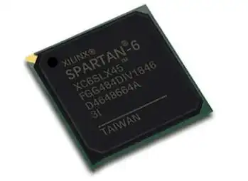
The XC6SLX45-3FGG484C is a top choice for embedded projects, offering exceptional processing power, versatile customization, and seamless integration. Engineers can take full advantage of the XC6SLX45-3FGG484C IC FPGA’s advanced features, such as:
-
High-speed interfaces, including PCI Express and 1G Ethernet, supporting data transfer rates up to 3.4 Gb per second
-
Extensive logic resources and adaptable clocking mechanisms for handling complex digital tasks
-
Frequency synthesis capabilities with phase shifting, division, and multiplication
The table below demonstrates why the XC6SLX45-3FGG484C IC FPGA is ideal for demanding applications:
|
Measure |
Value/Description |
|---|---|
|
Speed Grade |
2 (high-speed performance) |
|
RAM Size |
261 kB |
|
Package |
484-ball BGA |
|
Operating Voltage |
1.14V to 1.26V |
|
Operating Temperature |
0°C to 85°C |
|
Applications |
Digital signal processing, embedded systems |
Key Takeaways
-
The XC6SLX45-3FGG484C offers powerful processing with many logic cells and large on-chip memory, enabling fast and reliable handling of complex data.
-
Its highly programmable design lets engineers create custom digital circuits and quickly adapt to new features or standards.
-
With 316 input/output pins and a compact package, this FPGA supports many device connections while saving space on circuit boards.
-
The device runs efficiently within a stable voltage and temperature range, ensuring reliable performance in various environments.
-
Engineers can update designs remotely and securely, making it easy to improve systems without changing hardware.
Processing Power
Faster Data
The XC6SLX45-3FGG484C stands out with its impressive 43,661 logic cells and 3,411 configurable logic blocks. These resources allow the FPGA to process large amounts of data at high speeds. Engineers can design systems that handle real-time data streams without delays. The device’s architecture supports fast data movement, which is essential for applications like digital signal processing and high-speed communications.
The on-chip RAM, totaling 2,138,112 bits, gives the XC6SLX45-3FGG484C a strong advantage in data-intensive tasks. This memory allows the FPGA to store and access large data sets quickly. For example, other FPGAs with less RAM, such as the EP4CE40F29C8N, are already used in demanding fields like embedded vision, industrial automation, and robotics. The XC6SLX45-3FGG484C, with even more on-chip RAM, can handle even larger workloads and more complex buffering needs.
Note: The combination of high logic density and substantial RAM enables the XC6SLX45-3FGG484C to deliver fast and reliable data processing for advanced embedded projects.
Complex Tasks
The XC6SLX45-3FGG484C supports complex digital designs with its large number of logic cells and configurable logic blocks. Engineers can implement advanced algorithms, custom data paths, and specialized control systems. This flexibility makes the FPGA suitable for embedded control, where precise timing and quick responses are critical.
Many applications, such as medical devices and automotive electronics, require the ability to process and analyze data in real time. The XC6SLX45-3FGG484C meets these needs by providing both the speed and the memory needed for complex operations. Its architecture allows for parallel processing, which increases efficiency and reduces latency.
Customization with XC6SLX45-3FGG484C
Flexible Logic
Engineers often need to create systems with unique features or specialized functions. The XC6SLX45-3FGG484C makes this possible through its highly programmable architecture. The device contains 3,411 logic blocks and 43,661 programmable logic elements. These resources allow designers to build custom digital circuits that match the exact needs of their projects. Dedicated carry chains support modular design, while the adaptive clock distribution network ensures precise timing across different parts of the system.
The FPGA’s architecture supports massive parallel processing and complex logic customization. Designers can implement advanced algorithms, custom data paths, or unique control systems. The 316 configurable I/O channels with adaptive impedance matching provide flexible options for connecting to other devices. This flexibility proves valuable in fields like communication systems and embedded control, where requirements often change or evolve.
Tip: Modular design and programmable logic help engineers adapt quickly to new standards or protocols.
Some features that highlight the flexibility of FPGAs like the XC6SLX45-3FGG484C include:
-
Efficient 6-input lookup tables (LUTs) with dual flip-flops for pipeline-centric applications
-
Embedded high-performance arithmetic and signal processing blocks
-
Flexible granularity memory blocks for data storage and buffering
-
Multi-voltage, multi-standard I/O banks for signal integrity
Rapid Prototyping
The programmable nature of the XC6SLX45-3FGG484C supports fast prototyping and easy system upgrades. Engineers can quickly test new ideas or update existing designs without changing the hardware. The device’s MultiBoot support allows remote upgrades with multiple bitstreams and watchdog protection, making field updates simple and secure.
This rapid development cycle benefits industries that require frequent updates or custom solutions. Communication systems and embedded control applications often need to adapt to new protocols or features. The XC6SLX45-3FGG484C enables these changes with minimal downtime, helping teams stay ahead in fast-moving markets.
Reliable Integration
Extensive I/O
Engineers often need to connect many devices to a single system. The XC6SLX45-3FGG484C supports this need with 316 input/output pins. These pins allow the FPGA to communicate with sensors, displays, memory chips, and other peripherals. Designers can use these connections to build systems that gather data, control machines, or send information to other devices. The high pin count also helps when projects require multiple communication protocols or parallel data transfers.
Tip: More I/O pins mean greater flexibility for expanding or upgrading a project in the future.
The 484-ball FBGA package keeps the device compact. This small size saves space on the circuit board, making it easier to fit into tight enclosures or portable products. Engineers can design advanced systems without worrying about board space.
Stable Operation
Reliable performance matters in every embedded project. The XC6SLX45-3FGG484C operates within a supply voltage range of 1.14V to 1.26V. This efficient power range helps reduce energy use and heat generation. The device also works well in temperatures from 0°C to 85°C. This wide temperature range ensures stable operation in both commercial and industrial environments.
The table below compares the voltage and temperature ranges of similar FPGAs:
|
Device |
Supply Voltage Range |
Operating Temperature Range |
|---|---|---|
|
XC6SLX45-3FGG484C |
0°C – 85°C |
|
|
EP4CE40F29C8N |
0°C – 85°C |
|
|
XC6SLX75-3FGG484I |
1.14V – 1.26V |
-40°C – 100°C |
This table shows that the XC6SLX45-3FGG484C matches or exceeds the standards set by other leading FPGAs. Its robust voltage and temperature tolerance make it a strong choice for systems that must run reliably in changing conditions.
Note: The combination of a compact package, broad I/O support, and stable operation makes this FPGA ideal for demanding embedded and industrial applications.
Engineers gain three key benefits from this FPGA: strong processing power, flexible customization, and reliable integration. The device uses a mature 45 nm process, offers 3,411 configurable logic blocks, and supports advanced clock management. Its 484-FBGA package provides excellent EMI shielding and thermal management.
|
Feature Category |
Details |
|---|---|
|
Logic Resources |
43,661 logic cells, 3,411 CLBs |
|
Embedded Memory |
18 Kb block RAMs |
|
I/O Pins |
316 |
|
Serial Transceivers |
Up to 3.2 Gb/s |
|
Security Features |
AES encryption, Device DNA |
For more details, engineers can review datasheets, technical documents, and reference designs.
FAQ
What makes the XC6SLX45-3FGG484C suitable for embedded projects?
The XC6SLX45-3FGG484C offers high logic density, large on-chip RAM, and 316 I/O pins. These features help engineers build fast, flexible, and reliable embedded systems.
Can engineers update designs after deployment?
Yes. The FPGA supports remote upgrades with MultiBoot and watchdog protection. Engineers can update system features or fix bugs without replacing hardware.
How does the device handle different communication protocols?
The 316 I/O pins support multiple standards. Engineers can connect the FPGA to various peripherals, sensors, or networks. This flexibility helps in communication and control projects.
What is the operating temperature range for the XC6SLX45-3FGG484C?
The device operates from 0°C to 85°C. This range allows use in both commercial and industrial environments.
Does the XC6SLX45-3FGG484C support secure applications?
Yes. The FPGA includes AES encryption and Device DNA features. These security options help protect sensitive data and intellectual property.
See Also
Enhancing Automotive Performance Using MC9S12XEP100 And MC9S12XS128
Three Best Methods To Integrate MC9S12XET512VAG Effectively
Ways EP2C50F484I8N FPGA Can Revolutionize Your Projects
A Deep Dive Into MC9S12DJ256MFUE Specs For Automotives
Key Programming Fundamentals For MC9S12XD256 Microcontrollers