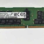
Modern embedded systems demand increased memory to handle complex tasks and larger datasets. The MT41K256M16TW DDR3 SDRAM provides a robust solution for these growing memory requirements. This specific component significantly enhances system performance, improves data handling capabilities, and boosts overall responsiveness. For projects leveraging advanced features, such as DDR3 4Gb SDRAM MT41K256M16TW FOR IoT and Communication Devices, selecting the right memory is critical. A reliable DDR3 distributor can also ensure access to authentic components. This guide offers practical steps, addresses potential challenges, and shares best practices for successful integration.
Key Takeaways
-
The MT41K256M16TW DDR3 SDRAM boosts embedded system performance. It offers high speed and low power use. This makes it good for many devices.
-
Proper hardware setup is key for the MT41K256M16TW. This includes careful circuit design and board layout. It also means managing power and signals well.
-
Software setup is important for the MT41K256M16TW. The memory controller needs correct timing and initialization. This ensures the memory works right with the system.
-
The MT41K256M16TW works in many devices. These include IoT gadgets, industrial systems, and networking gear. It helps them handle data better.
MT41K256M16TW: Features and Advantages
Core Specifications and Performance
The MT41K256M16TW DDR3 SDRAM stands out with its robust technical specifications. This memory IC offers a 4Gbit density, organized as 256M x 16, providing substantial storage capacity. It operates at a clock frequency of 933 MHz, translating to an effective data rate of 1866 MT/s. The component supports an 8-beat burst, which allows for efficient data transfer. Its low power operation at 1.35V makes it energy-efficient, though it maintains compatibility with 1.5V DDR3 systems. The access time is a swift 20 ns.
Here are the detailed specifications:
|
Specification |
Value |
|---|---|
|
Technology |
SDRAM – DDR3L |
|
Memory Size |
4Gbit |
|
Memory Organization |
256M x 16 |
|
Memory Interface |
Parallel |
|
Clock Frequency |
933 MHz |
|
Access Time |
20 ns |
|
Voltage – Supply |
1.283V ~ 1.45V |
|
Operating Temperature |
-40°C ~ 105°C (TC) |
|
Grade |
Automotive |
|
Qualification |
AEC-Q100 |
|
Mounting Type |
Surface Mount |
|
Package / Case |
96-TFBGA |
|
Supplier Device Package |
96-FBGA (8×14) |
|
Base Product Number |
MT41K256M16 |
Key Benefits for Embedded Designs
The MT41K256M16TW offers several advantages crucial for embedded systems. It provides high speed, significantly enhancing performance in demanding tasks. Its low power consumption makes it an excellent choice for battery-operated devices. The component ensures seamless integration with modern systems, providing reliable memory expansion.
Key benefits include:
-
High speed, significantly enhancing performance in demanding tasks.
-
Low power consumption, making it an excellent choice for battery-operated devices.
-
Seamless integration with modern systems, providing reliable memory expansion.
-
4Gb memory size, suitable for storing large amounts of data and meeting high DDR3 standards.
-
DDR technology for fast data transfers and burst read/write for smooth task execution.
-
Operates at 1.35V, contributing to energy saving, cooler device operation, and longer battery life.
-
Strong data transfer system ensuring smooth communication between memory and processor, with a clock speed of 933MHz, 20ns access time, and 16-bit data bus width.
Designers also appreciate its stable long-term supply, essential for products with extended lifecycles. The compact FBGA package saves valuable board space, and industrial temperature versions ensure reliability in harsh environments.
Pinout and Functional Overview
Understanding the pinout of the MT41K256M16TW is critical for proper hardware integration. This memory chip comes in a 96-FBGA (Fine-pitch Ball Grid Array) package. Each pin serves a specific function, including data lines, address lines, control signals, and power connections. Engineers must carefully map these pins to the memory controller on their embedded board. The functional overview shows it acts as a high-speed data buffer, storing and retrieving information for the main processor.
Diverse Applications of MT41K256M16TW DDR3 4Gb SDRAM
The MT41K256M16TW DDR3 4Gb SDRAM offers broad utility across many technology sectors. Its robust design and efficient performance make it a versatile choice for various demanding applications.
Embedded and Industrial Systems
This memory chip provides reliable operation for embedded and industrial systems. Engineers use it in Programmable Logic Controllers (PLCs) and Human-Machine Interfaces (HMIs). Industrial PCs and robotics also benefit from its stable performance. The MT41K256M16TW-107:P DDR3L SDRAM chip is designed for embedded systems. It also finds frequent use in servers and workstations for rapid memory operations. This makes it a robust option for many embedded applications. Furthermore, IoT gadgets and smart controllers often incorporate this memory. They require dependable memory for continuous data processing.
Computing and Networking Equipment
The MT41K256M16TW serves as main DRAM in compact computing and networking boards. Network routers and switches utilize this memory for high data throughput. Firewalls and gateways also rely on its stable operation. Single-board computers, including ARM or x86 SoCs, frequently integrate this DDR3 4Gb SDRAM. Its energy efficiency supports these devices well.
Optimizing for IoT and Communication Devices
The MT41K256M16TW is ideal for optimizing IoT and communication devices. IoT gateways and edge devices use this memory for local data buffering. Wireless baseband processors also benefit from its capabilities. Security cameras require efficient memory for image processing. The compact BGA package and low voltage make it suitable for space-constrained designs. This makes the DDR3 4Gb SDRAM MT41K256M16TW FOR IoT and Communication Devices a prime choice. Many designers select the DDR3 4Gb SDRAM MT41K256M16TW FOR IoT and Communication Devices. It provides essential memory for these systems. The DDR3 4Gb SDRAM MT41K256M16TW FOR IoT and Communication Devices ensures smooth data flow. This memory solution is critical for modern connected devices. The DDR3 4Gb SDRAM MT41K256M16TW FOR IoT and Communication Devices supports advanced functionalities.
Beyond these core areas, the MT41K256M16TW also finds use in automotive electronics. This includes infotainment systems and Advanced Driver-Assistance Systems (ADAS). Consumer electronics like Smart TVs and Digital Video Recorders (DVRs) also leverage its capabilities. This wide range of applications highlights the versatility of the MT41K256M16TW.
Hardware Integration: Connecting the MT41K256M16TW
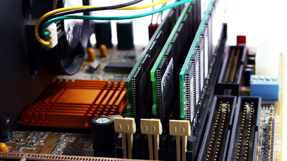
Integrating the MT41K256M16TW into an embedded design requires careful attention to hardware details. Proper schematic design, PCB layout, and signal integrity practices ensure optimal performance and reliability. Engineers must consider every aspect of the physical connection to achieve the full potential of this high-speed memory.
Schematic Design and Power Delivery
A precise schematic forms the foundation for successful memory integration. Designers must accurately connect all pins of the MT41K256M16TW to the memory controller and power rails. Power delivery is especially critical for high-speed DDR3 SDRAM. A stable and clean power supply prevents voltage fluctuations that can disrupt memory operations.
💡 Tip: A robust power delivery network (PDN) is essential for high-performance memory.
Engineers should follow specific guidelines for the power delivery network.
-
They utilize a stable power supply to prevent voltage fluctuations.
-
They position decoupling capacitors in close proximity to the power pins.
-
Decoupling capacitors are crucial for noise reduction and maintaining voltage stability.
These capacitors act as small reservoirs, providing instantaneous current when the memory chip demands it. This design minimizes power supply noise and ensures consistent voltage levels for reliable operation.
Signal Integrity and PCB Layout
Signal integrity is paramount when working with high-speed memory like DDR3 SDRAM. Poor signal integrity leads to data errors, reduced performance, and system instability. The physical layout of the Printed Circuit Board (PCB) directly impacts signal quality.
Designers must pay close attention to trace routing. They match the lengths of critical signal traces, such as data, address, and clock lines, to minimize skew. Skew occurs when signals arrive at different times, potentially causing timing violations. Using dedicated ground planes and power planes helps create a controlled impedance environment. This reduces electromagnetic interference (EMI) and crosstalk between adjacent traces. Careful routing practices prevent signal degradation and ensure reliable data transfer at high speeds.
Termination and Impedance Matching
Proper termination and impedance matching are vital for maintaining signal integrity in DDR3 interfaces. Without correct impedance matching, signals reflect back along the transmission line. These reflections cause signal distortion and can lead to data corruption.
For DDR3 SDRAM, both data and address lines necessitate a controlled impedance of 50 ohms. This specific impedance is crucial for maintaining signal integrity, minimizing reflections, and ensuring reliable high-speed data transfer within the memory system.
|
Line Type |
Impedance Requirement |
|---|---|
|
Data Lines |
Controlled impedance of 50 ohms |
|
Address Lines |
Controlled impedance of 50 ohms |
Engineers typically use series termination resistors or On-Die Termination (ODT) to match the impedance of the transmission lines to the source and receiver. This technique absorbs reflected signals, preventing them from interfering with subsequent data transmissions. Proper termination ensures clean signal waveforms and maximizes the effective data rate of the MT41K256M16TW. It is a critical step for achieving stable and high-performance memory operation.
Software Initialization and Memory Controller Setup
After connecting the MT41K256M16TW physically, engineers must configure the memory controller. This step involves software initialization and precise timing adjustments. Proper setup ensures the memory operates correctly and efficiently with the embedded system’s processor.
DDR3 Initialization Sequence
The DDR3 SDRAM requires a specific sequence of commands to become operational. This initialization process follows the JEDEC standard. The memory controller executes these steps during system power-up or reset.
Here are the typical steps in the DDR3 initialization sequence:
-
Power-Up and Reset: The system applies stable power to the DDR3 device. It then holds the
RESET#pin low for a specified duration. This ensures the memory starts in a known state. -
Clock Stabilization: The memory controller provides a stable clock signal to the DDR3. The clock must run for a minimum number of cycles before any commands are issued.
-
NOP Commands: The controller sends No Operation (NOP) commands. This allows the DDR3 device to stabilize internally.
-
Precharge All: The controller issues a
PRECHARGE ALLcommand. This closes all open memory banks. -
Mode Register Programming: The controller writes specific values to the DDR3’s Mode Registers (MR0, MR1, MR2, MR3). These registers configure various operational parameters.
-
MR0: Sets burst length, CAS latency, and wrap type.
-
MR1: Configures DLL enable/disable, output drive strength, and ODT (On-Die Termination) settings.
-
MR2: Defines write recovery time and self-refresh temperature range.
-
MR3: Sets the MPR (Multi-Purpose Register) operation.
-
-
DLL Enable: The controller enables the Delay Locked Loop (DLL). The DLL helps synchronize internal clock signals with the external clock. This step is crucial for high-speed operation.
-
ZQ Calibration: The controller performs ZQ calibration. This process fine-tunes the DDR3’s output driver impedance. It ensures optimal signal integrity.
-
Normal Operation: After these steps, the DDR3 SDRAM is ready for normal read and write operations.
💡 Note: Each step has specific timing requirements. The memory controller must adhere to these delays precisely. Failure to follow the sequence can lead to memory errors or system instability.
Timing Parameters and Calibration
DDR3 SDRAM relies on many critical timing parameters. These parameters define the delays between various memory operations. The memory controller must configure these values accurately. Examples include:
-
tCL(CAS Latency): The delay between a read command and data output. -
tRCD(RAS to CAS Delay): The time from an active command to a read/write command. -
tRP(Row Precharge Time): The time required to precharge a row. -
tRAS(Row Active Time): The minimum time a row must remain active. -
tRFC(Refresh Cycle Time): The time required for a refresh command.
The memory controller typically stores these parameters in its internal registers. The system firmware or bootloader loads these values during initialization.
Calibration is another vital process. It optimizes the timing and signal integrity of the DDR3 interface. Modern memory controllers often include built-in calibration engines. These engines perform:
-
Read Leveling: This adjusts the timing of the DQS (Data Strobe) signal relative to the clock. It ensures the memory controller samples read data correctly.
-
Write Leveling: This adjusts the timing of the DQS signal from the controller to the DDR3. It ensures the DDR3 receives write data correctly.
-
DQS Training: This process finds the optimal sampling window for data. It accounts for variations in PCB traces and component delays.
These calibration steps compensate for manufacturing variations and environmental factors. They ensure reliable data transfer at high speeds.
Driver Development and Memory Mapping
Software drivers enable the operating system or firmware to interact with the memory controller. These drivers configure the memory controller’s registers. They translate high-level memory requests into specific DDR3 commands.
A memory driver typically performs these functions:
-
Controller Configuration: It sets up the memory controller’s registers. This includes timing parameters, refresh rates, and power-saving modes.
-
Error Handling: It monitors for memory errors, such as ECC (Error-Correcting Code) errors. It reports these errors to the system.
-
Power Management: It manages the DDR3’s power states. This includes entering and exiting self-refresh mode to save power.
Memory mapping defines how the physical memory addresses of the DDR3 appear to the CPU. The memory controller handles this mapping. It presents a contiguous block of memory to the processor. The CPU then accesses this memory using virtual or physical addresses.
For example, a 4Gb (512MB) MT41K256M16TW device might map to a specific address range. The CPU sees this range as available for program code and data. The driver ensures that memory requests from the CPU correctly reach the DDR3 device. This seamless interaction allows applications to use the expanded memory effectively.
// Example (simplified) of memory controller register access
// This is illustrative and not actual code for a specific controller.

#define DDR_BASE_ADDR       0x10000000 // Base address of memory controller registers
#define DDR_MR0_REG         (DDR_BASE_ADDR + 0x00)
#define DDR_TIMING_REG1     (DDR_BASE_ADDR + 0x04)
#define DDR_CALIBRATION_CMD (DDR_BASE_ADDR + 0x08)

void configure_ddr_controller() {
    // Set Mode Register 0 (MR0) with desired burst length and CAS latency
    write_register(DDR_MR0_REG, 0x00001234); // Example value

    // Configure timing parameters (tCL, tRCD, tRP, etc.)
    write_register(DDR_TIMING_REG1, 0x56789ABC); // Example value

    // Initiate calibration sequence
    write_register(DDR_CALIBRATION_CMD, 0x00000001); // Start calibration

    // Wait for calibration to complete (e.g., poll a status register)
    while (read_register(DDR_CALIBRATION_CMD) & 0x00000002) {
        // Calibration in progress
    }
}
This code snippet shows how a driver might write to memory controller registers. It configures the DDR3 and initiates calibration. The driver acts as the bridge between the software and the hardware. It ensures the MT41K256M16TW operates as intended.
Ensuring Compatibility and Troubleshooting
Engineers must ensure compatibility and address potential issues for a successful MT41K256M16TW integration. This involves careful planning and systematic debugging.
Controller Compatibility and Speed Requirements
The memory controller plays a crucial role in the system. It must fully support the MT41K256M16TW. The memory controller needs to support DDR3L. It should also operate at 1.35V. Furthermore, the memory controller needs to handle a 16-bit data bus for optimal performance.
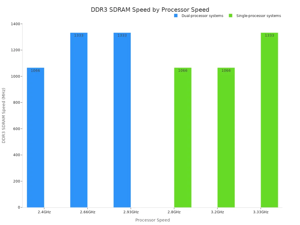
Different systems support various DDR3 SDRAM speeds. For example, dual-processor systems with a 2.4GHz processor often support 1066MHz DDR3 ECC SDRAM. Systems with 2.66GHz or 2.93GHz processors can handle 1333MHz. Single-processor systems also show varied speeds. A 2.8GHz processor typically supports 1066MHz, while 3.33GHz processors can use 1333MHz.
|
System Type |
Processor Speed |
DDR3 ECC SDRAM Speed |
|---|---|---|
|
Dual-processor systems |
2.4GHz |
1066MHz |
|
Dual-processor systems |
2.66GHz |
1333MHz |
|
Dual-processor systems |
2.93GHz |
1333MHz |
|
Single-processor systems |
2.8GHz |
1066MHz |
|
Single-processor systems |
3.2GHz |
1066MHz |
|
Single-processor systems |
3.33GHz |
1333MHz |
PUSKILL DDR3 desktop memory modules are available in 1333MHz and 1600MHz speeds. They are designed for PC RAM applications. Altera SoC FPGAs, specifically the Cyclone V family, feature hard memory controllers. These controllers support 400MHz DDR3 SDRAM. Their multiport SDRAM controller subsystem supports both DDR2 and DDR3 memory types.
Debugging Hardware and Software Issues
Debugging involves identifying and fixing problems. Hardware issues might include incorrect pin connections or power supply noise. Engineers use oscilloscopes to check signal integrity. Software issues often relate to incorrect timing parameters or initialization sequences. Debuggers help trace code execution and memory access.
Performance Optimization Strategies
Optimizing performance involves fine-tuning various settings. Adjusting timing parameters in the memory controller can improve speed. Enabling features like burst mode and on-die termination (ODT) also enhances data transfer. Regular calibration ensures the memory operates at its peak efficiency.
Integrating the MT41K256M16TW significantly enhances embedded system memory. It boosts performance and data handling. This guide covered crucial steps: hardware integration, software setup, and troubleshooting. Engineers should apply these best practices for reliable, high-performance memory solutions. This approach unlocks enhanced capabilities for embedded systems. 🚀
What is DDR3L and why is its low voltage important?
DDR3L is a low-voltage version of DDR3 SDRAM. It operates at 1.35V, consuming less power than standard 1.5V DDR3. This lower voltage helps embedded systems save energy. It also reduces heat generation, which extends battery life and improves device reliability.
How does the MT41K256M16TW improve embedded system performance?
The MT41K256M16TW offers 4Gb of memory and operates at high speeds, up to 1866 MT/s. This large capacity and fast data rate allow embedded systems to handle more complex tasks. It also processes larger datasets quickly, making the system more responsive and efficient.
What are key considerations for PCB layout with DDR3 SDRAM?
Engineers must ensure signal integrity. They match trace lengths for data, address, and clock lines to prevent timing issues. Using dedicated ground and power planes helps control impedance. This reduces noise and crosstalk, ensuring reliable high-speed data transfer.
Why is memory controller initialization crucial for DDR3?
The memory controller must follow a specific initialization sequence. This sequence configures the DDR3 SDRAM’s operational parameters. It includes setting timing values and enabling internal functions like the DLL. Correct initialization ensures the memory operates stably and efficiently with the processor.
See Also
EP2C50F484I8N FPGA: Bridging Theory and Practice for High-Performance Embedded Systems
MC9S12XEQ512CAL: Essential Specifications for This Powerful Microcontroller
Mastering Programming: Key Essentials for MC9S12XD256 Microcontroller Development
FREESCALE MCF5251CVM140: Unveiling Its Crucial Automotive Features and Benefits
MC9S12XET512VAG Microcontroller: Integrating Automotive Electronic Systems with Strategic Practices