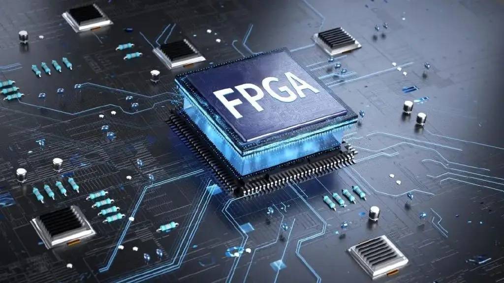
As an engineer with years of experience in the embedded systems field, I have personally witnessed how FPGAs have evolved from a “niche tool” in laboratories to becoming the core of high-performance, highly flexible system designs. Today, I would like to delve deeply into an FPGA that has demonstrated outstanding performance in practical projects – the EP2C50F484I8N from Intel’s (formerly Altera) Cyclone II series. This device not only inherits the inherent advantages of FPGAs but also strikes an excellent balance between performance and power consumption, providing engineers with vast space for innovation.
The Core Appeal of the EP2C50F484I8N FPGA
The essence of an FPGA lies in its “programmable” nature. Unlike fixed-function ASICs, FPGAs allow engineers to “reconfigure” at the hardware level, meaning we can update, optimize, or even completely change hardware functionality after product deployment. This flexibility is particularly valuable in the fast-iterating world of modern electronic design. The EP2C50F484I8N, as part of the Intel Altera Cyclone II family, stands out due to its:
-
Exceptional Performance-to-Power Ratio: Built on a 90nm process node, the EP2C50F484I8N delivers up to 60% higher performance than comparable devices while consuming only half the power. This is a decisive advantage for battery-powered applications or those with strict thermal requirements (such as portable medical devices, industrial control units). Low power consumption not only reduces operating costs but also simplifies thermal management design, enhancing system reliability.
-
Abundant Logic Resources & I/O: With 3,158 Logic Array Blocks (LABs), each containing multiple logic elements, it provides a solid foundation for implementing complex digital logic. Furthermore, up to 622 user I/O pins and 1.1 Mbits of embedded memory ensure its strong capability in handling high data throughput and multiple external interfaces. In a practical project, I leveraged its rich I/O resources to implement a multi-channel data acquisition system where each channel was independently configured, significantly simplifying the external interface circuit design.
-
True Parallel Processing Capability: This is one of the most significant differences between FPGAs and traditional microprocessors. Microprocessors typically execute instructions sequentially, whereas FPGAs enable genuine hardware-level parallel computation. For instance, in image processing, operations like filtering and edge detection can be performed simultaneously on different pixel blocks, dramatically increasing processing speed. This capability offers unparalleled advantages in applications demanding high real-time performance, such as digital signal processing (DSP) and encryption algorithms.
-
Dynamic Reconfigurability: Although the Cyclone II series does not support partial reconfiguration, its full reconfiguration capability remains powerful. This allows for updating or upgrading hardware functionality during the product’s lifecycle by downloading a new bitstream file, without needing to replace the physical chip. This provides immense convenience for extending product life, adapting to market changes, and fixing potential hardware flaws.
Practical Application Cases and Experience Sharing
These characteristics make the EP2C50F484I8N shine in several key fields. Below are some typical application scenarios and insights from my practical work:
1. Digital Signal Processing (DSP): The Core of Real-Time Performance
In radar signal processing or high-precision sensor data acquisition systems, the parallel processing capability of FPGAs is irreplaceable. I participated in an ultrasound imaging system project based on the EP2C50F484I8N. In this project, we needed to perform real-time sampling, filtering, FFT transformation, and beamforming on multiple channels of ultrasound signals. While traditional DSP chips could perform these tasks, they often struggled with processing speed and parallelism. Using the EP2C50F484I8N, we designed dedicated hardware accelerators, mapping each processing stage to independent logic resources for parallel execution, ultimately achieving a real-time imaging speed of hundreds of frames per second, far exceeding solutions based on general-purpose DSPs.
Experience Sharing: In DSP applications, rational planning of data flow and pipelining is crucial. Utilizing the FPGA’s Block RAM for high-speed caching, combined with its multiplier (M4K Block) resources, enables efficient implementation of complex algorithms like FIR/IIR filters and FFT. Simultaneously, pay close attention to setting timing constraints to ensure sufficient timing margin for high-speed data paths.
2. Software-Defined Radio (SDR): The Flexible Foundation of Communications
SDR is another “primary domain” for FPGAs. The reconfigurability of the EP2C50F484I8N enables radio systems to adapt to different communication protocols, modulation schemes, and frequencies via software updates. I used the EP2C50F484I8N on a small SDR platform to implement a multi-mode communication baseband processor. By loading different bitstreams, this platform could flexibly switch between supporting GSM, LTE, and even custom narrowband communication protocols. This flexibility significantly shortened the development cycle and reduced hardware costs.
Experience Sharing: In SDR design, the FPGA is primarily responsible for high-speed ADC/DAC interfaces, digital down/up conversion (DDC/DUC), channel filtering, modulation/demodulation, and other baseband processing. To improve code reusability, consider using HDL generation tools (like MATLAB HDL Coder) to convert algorithm models directly into HDL code. Additionally, properly utilizing the FPGA’s Phase-Locked Loop (PLL) resources to generate precise clocks is vital for the stability of the communication system.
3. Biomedical Instrumentation: Ensuring Precision and Reliability
Medical equipment demands extremely high precision, real-time performance, and reliability. The EP2C50F484I8N is widely used in medical imaging, physiological signal monitoring, and other fields. For example, in MRI (Magnetic Resonance Imaging) systems, vast amounts of RF signals need to be rapidly acquired and processed to reconstruct high-quality images. The high-speed I/O and parallel processing capabilities of the EP2C50F484I8N make it an ideal choice. It can process sensor data in real-time and execute complex algorithms, thereby improving diagnostic accuracy.
Experience Sharing: In medical FPGA designs, beyond technical performance, functional safety and reliability are paramount. During design, fully consider Error Detection and Correction (ECC) mechanisms, and perform rigorous functional verification and formal verification. Furthermore, low power consumption helps reduce device heating, improving patient comfort.
4. Encryption & Data Security: Fortifying the Digital Defense Line
In an era where data security is increasingly critical, FPGA applications in cryptography are becoming more widespread. The EP2C50F484I8N can be used to implement various encryption algorithms (e.g., AES, RSA, SHA), providing hardware acceleration. Because the FPGA’s hardware structure is configurable, it makes it difficult for attackers to crack the implementation details of the encryption algorithm through traditional software reverse engineering, thus enhancing security. In high-performance network security equipment, I used the EP2C50F484I8N to implement a hardware encryption module for real-time encryption/decryption of high-speed data streams, ensuring data confidentiality and integrity.
Experience Sharing: Encryption algorithms often involve extensive bit manipulations and mathematical operations. Leveraging the FPGA’s Look-Up Tables (LUTs) and dedicated multiplier resources allows for efficient implementation of these algorithms. To prevent side-channel attacks, pay attention to power consumption and electromagnetic radiation uniformity during design, and consider incorporating security modules like True Random Number Generators.

Key Elements for EP2C50F484I8N Project Implementation
Successfully applying the EP2C50F484I8N to real-world projects requires a robust development process and toolchain. As engineers, we understand the importance of using the right tools.
1. Development Tools: Intel Quartus Prime Software
Intel Quartus Prime (formerly Altera Quartus II) is the official Integrated Development Environment (IDE) for developing Altera FPGAs. It provides a complete workflow from design entry, synthesis, place-and-route, timing analysis, to device programming. For the EP2C50F484I8N, we need to use a Quartus version that supports the Cyclone II series. Its powerful simulator and debug tools (like the SignalTap II Logic Analyzer) are crucial for locating and resolving design issues.
Practical Advice:
-
Project Setup: When creating a new project, be sure to correctly select the target device family (Cyclone II) and specific device (EP2C50F484I8N). This affects subsequent pin assignment and timing analysis.
-
Design Entry: Using Hardware Description Languages (HDL) like Verilog or VHDL is recommended. For complex control logic, consider using state machine diagrams or IP cores.
-
Timing Analysis: The Quartus Timing Analyzer (TimeQuest) is key to ensuring the design operates stably at the target frequency. Learning to interpret timing reports and adjust the design or constraints based on them is an essential skill for every FPGA engineer.
-
Debugging: SignalTap II allows real-time capture of internal FPGA signals without affecting design functionality. This is extremely useful for debugging complex logic and verifying data flows.
2. Hardware Support: Development Boards & Peripherals
Selecting a suitable development board is the starting point for project success. There are many development boards based on the Cyclone II series available on the market, typically integrating power management, JTAG download interfaces, clock sources, and various peripheral interfaces (e.g., VGA, LCD, Ethernet, SD card). When choosing, ensure the board provides sufficient resources and is easy to expand based on project requirements.
Practical Advice:
-
Power Integrity: FPGAs are sensitive to power supply noise. When designing your own PCB, pay strict attention to power decoupling and ground plane design.
-
Clock Management: Select clock sources with low jitter and high stability. For multi-clock domain designs, pay special attention to Clock Domain Crossing (CDC) handling to avoid metastability issues.
-
Pin Assignment: Carefully read the EP2C50F484I8N datasheet to understand the functionality and electrical characteristics of different pins. Allocate I/O pins rationally to avoid signal integrity problems.
3. Programming Steps: From HDL to Bitstream
-
Create Project & Add Source Files: Create a new project in Quartus Prime and add your Verilog/VHDL design files.
-
Set Pin Assignments: Map the I/O ports in your design to the physical pins of the EP2C50F484I8N according to the development board or custom PCB schematic.
-
Compile the Design: Run the Full Compilation (Analysis & Synthesis, Fitter, Assembler, Timing Analyzer). This process converts the HDL code into a gate-level netlist, performs place-and-route, and generates timing reports.
-
Verify Timing: Check the timing report to ensure all critical paths meet timing requirements. If not, optimize the HDL code or adjust timing constraints.
-
Generate Programming File: If compilation and timing verification pass, Quartus will generate programming files like
.sof(SRAM Object File) or.pof(Programmer Object File). The.soffile is used for downloading to the FPGA’s SRAM via the JTAG interface (volatile); the.poffile is used for programming an external configuration memory device (e.g., EPCS) for non-volatile storage. -
Download & Verify: Use a downloader like the USB-Blaster to transfer the programming file to the EP2C50F484I8N via the JTAG interface. After power-up, verify that the design functions as expected.
Looking Ahead: The Continuous Evolution of FPGAs
Although the EP2C50F484I8N is an earlier product, its classic design philosophy and exceptional performance still hold unique value today. It is not only an excellent choice for engineers starting with FPGAs but also remains active in industrial control, communications, and medical fields with strict cost, power, and reliability requirements. With the rise of heterogeneous computing, AI acceleration, and edge computing, the role of FPGAs as hardware accelerators is becoming increasingly important. Mastering the design and application of classic FPGAs like the EP2C50F484I8N undoubtedly lays a solid foundation for understanding more advanced FPGA architectures and tackling future design challenges.
As engineers, we must not only focus on the latest technologies but also deeply understand the design philosophy and application essence of classic devices. The EP2C50F484I8N is precisely such a paradigm, continuously empowering countless innovative projects with its powerful features and flexible characteristics. I hope my experience sharing provides you with inspiration as we explore the infinite possibilities of the FPGA world together!
References:
[1] Altera Cyclone II Device Handbook. (Available on Intel FPGA official website).
[2] Intel Quartus Prime Software Documentation. (Available on Intel FPGA official website).
See Also
Revolutionizing Industrial Automation with ATIC83E2 in 3 Ways
Best Practices for Integrating MC9S12XET512VAG in 3 Ways
The Impact of XCF01SVOG20C on Industrial Automation: Top 3 Changes
Diving into MC9S12DJ256MFUE Specs for Automotive Use Cases
Essential R5F64219JFB Features for High-Quality Audio Gear

