
Integrating the VCNL4040M3OE sensor into modern consumer electronics unlocks advanced ambient and proximity sensing in even the smallest devices. The VCNL4040M3OE combines ambient light detection and proximity measurement, making it ideal for mobile devices that require precise screen brightness adjustment and user detection.
Recent trends show strong growth in sensor adoption across smart devices:
Miniaturization and easy integration drive seamless integration in wearables and handhelds.
Multi-modal sensors, including ambient and light sensors, support smarter device experiences.
The global consumer electronics sensor market is projected to reach over $90 billion by 2034.
Correct hardware and software setup ensures optimal sensor performance. Developers can achieve easy integration and reliable results by following best practices for sensor placement, calibration, and signal management.
Key Takeaways
-
Choose the VCNL4040M3OE sensor based on your device’s needs, considering size, power use, and sensing accuracy for ambient light and proximity.
-
Connect the sensor properly using the I2C interface and ensure correct power supply and pin wiring to avoid communication errors.
-
Set up the sensor software by initializing registers, using interrupts, and calibrating for accurate and stable measurements.
-
Manage power wisely by using low-power modes and interrupts to extend battery life in mobile devices.
-
Test and troubleshoot carefully by checking connections, cleaning the sensor window, and validating sensor data to ensure reliable performance.
VCNL4040M3OE Sensor Selection
Application Fit
Selecting the right sensor for a device starts with understanding the intended application. The VCNL4040M3OE suits a wide range of electronic products, from smartphones to smart home devices. Developers should consider how the sensor will support features like automatic screen brightness, proximity detection, or gesture control. Each application may require different levels of high sensitivity, accuracy, and response time. For example, a digital ambient light sensor in a tablet must quickly adjust display brightness in changing lighting conditions. In contrast, a proximity sensor in a wearable device needs to detect user presence with minimal power use.
Objective criteria help guide sensor selection. These include validity, reliability, sensitivity, specificity, and the ability to detect and differentiate changes in the environment. Developers often use a checklist to score each parameter, making it easier to compare sensors for a specific application. Usability factors such as size, weight, ease of use, and power consumption also play a major role. The VCNL4040M3OE, with its compact size and high sensitivity, fits well in space-limited consumer electronics.
Tip: Visualization tools like spider charts can help compare sensor specifications across multiple parameters, making the selection process more efficient.
Compatibility Factors
Compatibility ensures that the sensor works smoothly with the rest of the electronic system. Developers should check the voltage range, communication interface, and physical dimensions of the VCNL4040M3OE. This sensor operates on a 2.5V–3.6V supply and uses an I2C interface, which matches most modern microcontrollers. The small package size allows easy integration into compact electronic designs.
Ambient light sensors must also match the optical requirements of the application. The VCNL4040M3OE uses Filtron technology for visually accurate ambient light measurement, supporting both high sensitivity and precise readings. Developers should review the sensor specifications to confirm that the device meets the sampling rate and power needs of their application. Cleaning and maintenance requirements, as well as environmental toughness, should also be considered for long-term reliability.
A systematic evaluation, driven by the application, helps balance measurement accuracy, usability, and design. This approach ensures that the selected sensor delivers optimal performance in real-world consumer electronics.
Hardware Integration
Pinout and Connections
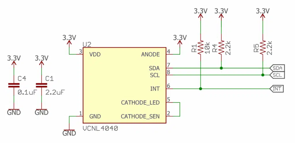
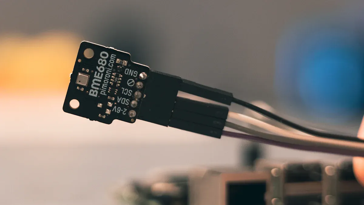
Integrating the VCNL4040M3OE sensor into an electronic device starts with understanding its pinout and connections. The sensor uses a compact package, which fits well in space-limited designs. It operates within a voltage range of 2.5V to 3.6V, making it compatible with most modern microcontrollers. The I2C interface allows for efficient communication with the main processor.
The following table shows common pin and signal functions for connecting sensors like the VCNL4040M3OE to a microcontroller such as the Arduino Nano:
|
Interface |
Pin/Signal |
Function/Description |
|---|---|---|
|
Arduino Nano |
3.3V |
Provides steady 3.3 volts power output for sensors requiring this voltage. |
|
Digital I/O |
General-purpose input/output pins for connecting sensors or devices, configurable as input or output. |
|
|
Analog Input |
Reads varying voltage levels from analog sensors (e.g., temperature, light intensity). |
|
|
I2C (SDA, SCL) |
Two-wire communication interface for connecting multiple sensors and devices efficiently. |
The VCNL4040M3OE connects to the I2C lines (SDA and SCL) for data transfer. Developers should ensure that the sensor’s power and ground pins connect to the correct supply rails. Proper pinout connections support reliable sensor operation and prevent communication errors.
Light Sensor Electronic Circuits
The VCNL4040M3OE uses advanced light sensor electronic circuits to achieve high sensitivity and high accuracy in both proximity and ambient light measurements. The sensor features a 3D CMOS-fabricated photodiode with multiple PN junctions. This structure reduces dark current and substrate noise, which improves the signal quality.
|
Aspect |
Description |
|---|---|
|
Photodiode Structure |
3D CMOS-fabricated photodiode with multiple PN junctions to reduce dark current and substrate noise |
|
Operating Principle |
Photogenerated carriers form stable photocurrent under illumination; verified by electric field and current density simulations |
|
Simulation Results |
Electric field strength concentrated at PN junction (~2.7 × 10^5 V/cm); I-V characteristics show clear difference between dark and illuminated conditions |
|
Dark Current Compensation Circuit |
Programmable circuit with selectable gain modes (High: 100,000; Medium: 10,000; Low: 1,000) to suppress dark current effects |
|
Experimental Fabrication |
Chip fabricated using 0.18 µm CMOS process; layout and micrographs confirm practical implementation |
|
Measurement Results |
Output current linearly increases with light intensity from 0 lux to 100 K lux across gain modes; power supply current also shows linear response |
|
Dynamic Range & Linearity |
Wide dynamic range (0 to 100 K lux) with good linearity demonstrated by experimental data |
The sensor’s light sensor electronic circuits include a programmable dark current compensation circuit. This feature allows the sensor to maintain accuracy across different lighting conditions. The output current increases linearly with light intensity, which supports precise ambient light sensor readings. The sensor’s circuits also support low power consumption, which is important for battery-powered devices.
PCB Layout
A well-designed PCB layout ensures optimal sensor performance and minimizes noise. The VCNL4040M3OE benefits from careful placement of passive components and thoughtful routing of traces.
-
Select stable, low-noise capacitors such as polystyrene or surface mount NPO/COG ceramics for filtering.
-
Place 0.1-μF ceramic bypass capacitors close to each supply pin to reduce noise coupling.
-
Separate analog and digital grounds physically and dedicate PCB layers to ground planes.
-
Route input traces away from supply or output traces to reduce parasitic coupling. If crossing is necessary, do so perpendicularly.
-
Place external components close to the sensor to minimize parasitic capacitance.
-
Keep input trace lengths as short as possible to reduce noise pickup.
-
Consider a low-impedance guard ring around critical traces to reduce leakage currents.
Sensor placement also affects accuracy. Developers should mount the sensor so that the light path is unobstructed. Cleaning the sensor window and avoiding dust buildup help maintain consistent readings. Avoid placing the sensor near strong light sources or high-frequency circuits to reduce interference.
Tip: Use a dedicated ground plane and keep the sensor away from noisy digital circuits for best results.
Power and Signal
Power and signal configuration play a key role in the VCNL4040M3OE’s performance. The sensor supports low power consumption, which extends battery life in portable devices. The I2C interface enables efficient data transfer with minimal wiring.
The following table summarizes important aspects of power and signal configuration:
|
Aspect |
Measurement Data / Technical Detail |
Impact on Sensor Performance |
|---|---|---|
|
ADC reference voltage developed from excitation current; system accuracy insensitive to excitation variations (~1% current tolerance). |
Ensures measurement accuracy independent of excitation source stability. |
|
|
AC vs DC Excitation |
AC excitation reduces noise, offset, and self-heating; chopping at asynchronous 57 Hz reduces line-frequency pickup noise. |
Improves signal-to-noise ratio, reduces offset drift, and minimizes self-heating errors in resistive sensors. |
|
Wiring Configurations |
2-wire: lead resistance adds significant error (e.g., 1 Ω leads to ~2.6°C error in 100 Ω RTD). 3-wire: halves error by eliminating one lead current. 4-wire: eliminates lead resistance errors entirely. |
4-wire configuration provides highest accuracy by removing lead wire resistance and thermal effect errors. |
|
Chopper Stabilization |
Use of chopper mode in AD7730 reduces offset drift to <5 nV/°C and maintains flat offset in presence of electric fields (1-3 V/m, 30 MHz-1 GHz). |
Minimizes offset drift and noise in electrically noisy environments, enhancing measurement stability. |
|
Excitation Magnitude |
Must be sufficient to produce output changes above noise and offset; AC excitation allows lower excitation reducing self-heating. |
Balances resolution and sensor self-heating, improving measurement reliability and sensor longevity. |
The VCNL4040M3OE includes an interrupt function, which helps reduce power use by waking the main processor only when a threshold is crossed. This feature supports low power consumption and efficient operation in mobile devices. Developers should configure the I2C interface for reliable communication and use proper wiring techniques to minimize signal loss.
The sensor’s light sensor electronic circuits, combined with careful power and signal management, deliver high sensitivity and stable performance in a wide range of electronic applications.
Software Integration Strategies
I2C Setup
A robust I2C setup forms the backbone of reliable sensor communication in electronic devices. The VCNL4040M3OE uses the I2C protocol, which simplifies wiring and supports easy integration with microcontrollers. I2C uses only two lines—SDA for data and SCL for the clock—plus a common ground. This setup reduces wiring complexity in compact electronic designs.
Key best practices for I2C setup include:
-
I2C bus drivers use open-drain outputs. These prevent bus contention and damage by only pulling lines low, while pull-up resistors restore the high state.
-
Pull-up resistors on SDA and SCL lines are essential. A typical value is 4.7kΩ, but this can be adjusted based on bus length and the number of devices.
-
For longer bus runs or more devices, smaller pull-up resistor values improve signal integrity.
-
Many sensors include onboard pull-up resistors. When multiple devices share a bus, some pull-ups may need to be disconnected to optimize total resistance.
-
The I2C bus can support about seven devices without issues. For more devices, resistor adjustments or bus extenders may be necessary.
-
For extended cable lengths, dedicated ICs like the PCA9615 I2C bus extender help maintain signal quality.
-
I2C allows some voltage level flexibility, but level shifters are recommended for mixed-voltage systems.
Tip: Always check the sensor datasheet for recommended pull-up resistor values and bus configuration.
This approach ensures stable communication and supports high-performance sensor integration strategies in modern electronic systems.
Sensor Initialization
Proper sensor initialization is critical for accurate ambient and proximity measurements. The VCNL4040M3OE requires a sequence of commands to configure its registers and prepare it for operation. Developers should use available libraries or APIs to streamline this process and reduce errors.
The initialization process involves:
-
Powering up the sensor and verifying communication over I2C.
-
Configuring the sensor’s registers for ambient light and proximity modes.
-
Setting up interrupt thresholds for efficient event handling.
-
Synchronizing the sensor’s internal reference and measurement circuits to ensure stable output.
Reference designs show that optimal sensor start-up procedures rely on precise, synchronized initialization of sensor and reference circuits. This synchronization compensates for temperature drift and ensures reliable performance. Adjusting parameters such as capacitance and junction area can enhance sensitivity, but these changes must balance device size and stability.
Here is a sample code snippet for initializing the VCNL4040M3OE using a common microcontroller platform:
// Example: VCNL4040M3OE Initialization (Arduino-style pseudocode)
Wire.begin();
writeRegister(VCNL4040_COMMAND, AMBIENT_LIGHT_ENABLE | PROXIMITY_ENABLE);
writeRegister(VCNL4040_ALS_CONF, ALS_IT_80MS | ALS_PERS_1);
writeRegister(VCNL4040_PS_CONF, PS_IT_8T | PS_PERS_1);
Note: Use manufacturer-provided libraries for easy integration and to avoid low-level errors.
Data Acquisition
After initialization, the sensor begins collecting ambient and proximity data. The VCNL4040M3OE supports real-time data acquisition through its I2C interface. Developers can read sensor output at regular intervals or use interrupts for event-driven data collection.
Best practices for data acquisition include:
-
Polling the sensor at a fixed interval for continuous monitoring.
-
Using the sensor’s interrupt function to trigger data reads only when thresholds are crossed, reducing power consumption.
-
Storing raw data in buffers for later processing or immediate use.
-
Filtering and averaging data to reduce noise and improve measurement stability.
A typical data acquisition loop might look like this:
// Example: Reading ambient and proximity data
uint16_t ambient = readRegister(VCNL4040_ALS_DATA);
uint16_t proximity = readRegister(VCNL4040_PS_DATA);
// Process or display the data as needed
Developers should validate the output against expected ranges to ensure sensor health and system reliability.
Calibration
Calibration ensures that the sensor delivers accurate and consistent measurements in different environments. The VCNL4040M3OE supports both ambient light and proximity calibration. Developers should follow a structured calibration process to optimize sensor performance.
Key calibration steps include:
-
Zero calibration: Expose the sensor to a zero-level input to correct offset or bias.
-
Span calibration: Use a known maximum input to scale the output correctly across the sensor’s range.
-
Linearity assessment: Test how well the sensor output corresponds to input values across the operational range. Apply calibration curves or mathematical models to correct deviations.
Comparative analysis of calibration models shows that simple algorithms like linear regression offer computational efficiency and reasonable precision. More complex models, such as random forest or neural networks, provide higher accuracy but require more data and resources. Environmental factors like temperature and humidity can affect sensor performance, so calibration should consider these variables.
Establishing clear performance targets and benchmarks improves data quality and builds confidence in sensor-based electronic systems.
A well-calibrated sensor ensures reliable ambient and proximity readings, supporting advanced integration strategies and high-quality user experiences.
System-Level Integration
Power Management
Effective power management ensures that devices with the VCNL4040M3OE sensor operate efficiently and reliably. Engineers monitor energy use in real time and use data analytics to adjust consumption. They often apply load management techniques, such as load shifting and peak shaving, to optimize energy use and reduce stress on the power grid. Devices must operate within safe voltage and current ranges, usually between 2.5V and 3.6V for this sensor, to maintain efficiency and safety.
Key strategies for power management include:
-
Using real-time monitoring to adjust energy use dynamically.
-
Applying load management to balance power consumption.
-
Tracking power consumption and efficiency metrics to guide decisions.
-
Integrating IoT and energy management systems for coordinated control.
-
Using predictive maintenance to extend device lifespan and reduce failures.
A table of common metrics:
|
Metric |
Description |
|---|---|
|
Power Consumption |
Measures energy use over time (watts/milliwatts) |
|
Efficiency |
Ratio of useful output to total input |
|
Operating Voltage |
Safe voltage range for device operation |
These strategies help engineers minimize costs and emissions while maintaining device performance.
Mobile OS Interface
Mobile operating systems play a key role in sensor data collection and user experience. Studies show that sensor accuracy can vary between devices and operating systems. Native apps, which run directly on the OS, often collect data more reliably than web apps. Data collection rates differ between Android and iOS, with Android devices reporting slightly higher rates. Technical solutions, such as push notifications and conditional sensor activation, improve data completeness and conserve battery life.
Battery consumption remains a concern. For example, scanning every five minutes can reduce battery life by about 12%. Adjusting scanning intervals and activating sensors only when needed can help manage this impact. Device models also influence data completeness, so engineers must test across multiple platforms to ensure consistent performance.
Mobile OS interfaces must support efficient data acquisition and battery management to deliver a seamless user experience.
EMC/EMI Considerations
Electromagnetic compatibility (EMC) and electromagnetic interference (EMI) affect sensor reliability in electronic devices. Empirical research has established sensitivity thresholds for sensors using criteria like interference margins and bit error rates. Engineers use EMC prediction software and testing tools to identify and mitigate potential issues.
Key practices include:
-
Measuring emissions and immunity of both modules and assembled systems.
-
Classifying immunity levels based on system criticality and performance.
-
Testing across a wide frequency range, including voltage drop-outs and electrostatic discharge (ESD).
-
Improving EMI filter design through impedance mismatching and careful layout.
These steps ensure that sensors like the VCNL4040M3OE maintain robust performance even in complex electromagnetic environments. Continuous testing and validation help engineers deliver reliable consumer and mobile devices.
Testing and Troubleshooting
Common Issues
Engineers often encounter several common issues when integrating the VCNL4040M3OE sensor into electronic devices. Incorrect wiring or loose connections can cause the sensor to fail to communicate with the microcontroller. If the sensor sits too close to strong light sources, it may produce inaccurate ambient readings. Dust or fingerprints on the sensor window can block light and reduce sensitivity. Sometimes, the sensor may not trigger interrupts as expected if thresholds are not set correctly. Power supply noise or voltage drops can also affect sensor performance.
Tip: Always check the sensor’s orientation and ensure the window remains clean for accurate detection.
Debugging
Debugging sensor integration requires a systematic approach. Engineers start by verifying all electronic connections and confirming the correct voltage supply. They use I2C scanners to detect if the microcontroller recognizes the sensor address. Reading raw data from the sensor registers helps identify if the ambient and proximity functions work as intended. If the sensor does not respond, engineers check for software errors in initialization or data acquisition routines. They may use an oscilloscope to monitor I2C signals and confirm stable communication. Adjusting interrupt thresholds and testing with different light levels can help fine-tune sensitivity.
A simple debugging checklist:
-
Confirm power and ground connections.
-
Scan for the sensor’s I2C address.
-
Read and log sensor data.
-
Test with varying ambient light conditions.
-
Adjust interrupt settings and observe responses.
Performance Validation
Performance validation ensures the sensor operates reliably in the final electronic system. Engineers define requirements based on device features, such as the need for accurate detection of ambient light or proximity. They experiment with sensor placement to optimize field of view and minimize blind spots. Simulations and real-world tests help evaluate sensor accuracy, range, and sensitivity.
Key performance metrics include:
-
Accuracy and precision: Measure how closely sensor readings match actual light levels.
-
Sensitivity: Assess the sensor’s ability to detect small changes in ambient conditions.
-
False positive rate: Track how often the sensor triggers incorrect events.
-
Response time: Record how quickly the sensor reacts to changes.
-
Robustness: Test the sensor’s resilience to environmental factors like temperature or electrical noise.
-
Energy efficiency: Monitor power consumption during operation.
Engineers use these metrics to compare sensor performance against system requirements. This process helps optimize sensor configuration and ensures reliable operation in electronic devices.
The VCNL4040M3OE sensor offers reliable proximity and ambient light sensing for any compact device. Engineers can achieve optimal results by following best practices for hardware and software integration. They should consult datasheets and application notes for deeper insights. Prototyping with evaluation boards helps validate designs. Joining developer communities provides valuable support and shared experiences.
How does the VCNL4040M3OE sensor connect to a microcontroller?
The VCNL4040M3OE uses an I2C interface. Developers connect the sensor’s SDA and SCL pins to the microcontroller’s I2C lines. Power and ground pins must also connect to the correct voltage rails for stable operation.
Can the VCNL4040M3OE detect hand gestures or simple movements?
Yes. The VCNL4040M3OE can detect basic hand gestures or movements near the sensor. Many consumer devices use this feature for wake-on-approach or gesture-based controls. It works well alongside other motion and position sensors for enhanced user interaction.
What is the recommended placement for the VCNL4040M3OE in a device?
Engineers should place the sensor where light can reach it without obstruction. Avoid placing it near strong light sources or high-frequency circuits. Keeping the sensor window clean ensures accurate ambient and proximity readings.
Does the VCNL4040M3OE support low-power operation?
The VCNL4040M3OE supports low-power modes. Developers can use the interrupt function to wake the main processor only when needed. This feature helps extend battery life in portable devices.
How do engineers calibrate the VCNL4040M3OE for different environments?
Engineers perform zero and span calibration using known light and proximity values. They may also test the sensor in various lighting conditions. Calibration ensures the sensor provides accurate and consistent data in real-world applications.
See Also
Simple Steps To Integrate Sensors With SN74LVC4245APW
Three Best Methods For Integrating MC9S12XET512VAG
How To Use ADXL357BEZ For Motion Sensors And Stability
Detailed Overview Of MC9S12DJ256MFUE Specs For Vehicles
AD9736BBCZ Leading Innovations In Wireless Communication