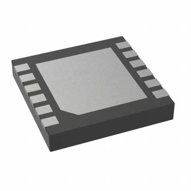
Efficient power delivery is critical for FPGA and ASIC systems, where performance depends on stable voltage regulation. The MAX20058ATCA/VY+T plays a pivotal role in addressing these demands. Its wide input voltage range of 4.5V to 60V and excellent voltage regulation make it a reliable choice for powering high-performance components.
Modern applications face challenges like dynamic voltage demands and thermal hotspots. These issues can lead to performance throttling or physical damage. By offering high efficiency and synchronous step-down DC-DC conversion, the MAX20058ATCA/VY+T ensures consistent power delivery while minimizing energy wastage. This blog provides a detailed guide to integrating this advanced IC into FPGA and ASIC systems.
Key Takeaways
-
The MAX20058ATCA/VY+T works well for FPGA and ASIC systems. It supports input voltages from 4.5V to 60V, making it flexible for different power sources.
-
It saves energy with high efficiency and step-down conversion. This reduces heat and makes the system more reliable.
-
Checking power needs is very important. Look at core voltage, extra power needs, and changes during use to keep it working well.
-
Picking the right parts, like low ESR capacitors and good inductors, helps it run smoothly and efficiently.
-
Testing and checking power delivery and system stability are key. This ensures the MAX20058ATCA/VY+T works for your project.
Understanding the MAX20058ATCA/VY+T
Key Features and Specifications
The MAX20058ATCA/VY+T is a high-efficiency DC-DC buck converter designed to meet the demanding power requirements of modern systems. Its specifications make it a versatile choice for applications requiring precise voltage regulation and robust performance.
|
Parameter |
Value |
|---|---|
|
Input Voltage Range |
4.5V to 60V |
|
Output Voltage |
800 mV to 54 V |
|
Output Current |
1 A |
|
Switching Frequency |
200 kHz to 2.2 MHz |
|
Operating Temperature |
-40°C to +125°C |
|
Qualification |
AEC-Q100 |
This IC offers a wide input voltage range, making it adaptable to various power sources. Its programmable output voltage and high switching frequency provide flexibility for different applications. The AEC-Q100 qualification ensures reliability in automotive and industrial environments.
Benefits for FPGA and ASIC Power Systems
The MAX20058ATCA/VY+T delivers several advantages for FPGA and ASIC power systems. Its high efficiency minimizes energy loss, reducing heat generation and improving overall system reliability. The wide input voltage range (4.5V to 60V) supports diverse power supply configurations, while the programmable output voltage ensures compatibility with the specific needs of FPGAs and ASICs.
This IC’s ability to deliver up to 1A of current makes it suitable for powering multiple components within FPGA and ASIC designs. Its feedback voltage-regulation accuracy of ±1.5% across a temperature range of -40°C to +125°C ensures stable operation even in challenging environments. These features help maintain consistent performance, which is critical for applications like telecommunications, data centers, and industrial automation.
By integrating the MAX20058ATCA/VY+T, designers can achieve precise voltage regulation and robust thermal performance. This makes it an ideal choice for powering high-performance FPGA and ASIC systems.
Preparing for Integration
Assessing FPGA/ASIC Power Requirements
Before integrating the MAX20058ATCA/VY+T, designers must evaluate the power requirements of their FPGA or ASIC system. This step ensures compatibility and optimal performance. Each FPGA or ASIC has unique voltage and current demands based on its architecture and workload. Designers should consult the datasheets and technical documentation of their target device to identify these parameters.
Key factors to consider include:
-
Core Voltage Requirements: Determine the operating voltage range for the FPGA or ASIC core.
-
Peripheral Power Needs: Assess the power demands of connected peripherals, such as memory modules or communication interfaces.
-
Dynamic Power Variations: Account for fluctuations in power consumption during different operational states.
Accurate power profiling helps prevent underpowering or overdesigning the system. Tools like power estimation software or hardware measurement instruments can assist in this process.
Selecting External Components for MAX20058ATCA/VY+T
The MAX20058ATCA/VY+T requires external components to function effectively. Selecting the right components ensures stable operation and maximizes efficiency.
-
Input Capacitors: Choose capacitors with low equivalent series resistance (ESR) to handle input voltage fluctuations.
-
Output Capacitors: Select capacitors that provide sufficient filtering to maintain a stable output voltage.
-
Inductors: Use inductors with appropriate current ratings and low core losses to support the desired output current.
-
Feedback Resistors: Configure the feedback network to set the desired output voltage.
-
Diodes (if applicable): For certain configurations, Schottky diodes may be required to improve efficiency.
Component selection should align with the specifications outlined in the MAX20058ATCA/VY+T datasheet. Proper selection reduces noise, enhances thermal performance, and ensures reliable power delivery.
Tip: Always verify component ratings against the operating conditions of the target application to avoid failures.
Integration Process for MAX20058ATCA/VY+T
Designing the Power Supply Circuit
Designing a power supply circuit for the MAX20058ATCA/VY+T involves careful planning to ensure stable and efficient operation. The process begins with determining the input voltage range and output voltage requirements. These parameters depend on the target application, such as FPGA or ASIC systems.
Next, designers must select the appropriate external components. Input capacitors should handle voltage fluctuations effectively, while output capacitors must provide sufficient filtering to maintain a stable output. Inductors with low core losses and suitable current ratings are essential for supporting the desired output current. Feedback resistors play a critical role in setting the output voltage, ensuring compatibility with the system’s power needs.
Proper placement of these components on the PCB minimizes noise and enhances thermal performance. Designers should also consider the switching frequency, as it impacts efficiency and component selection. A higher frequency allows for smaller components but may increase power loss.
Tip: Use simulation tools to validate the circuit design before implementation. This step helps identify potential issues and optimize performance.
Configuring the IC for Application Needs
Configuring the MAX20058ATCA/VY+T for specific applications requires precision and the right tools. The EE-Sim Power® Tools simplify this process by enabling designers to create complete power designs, including schematics and simulations. These tools allow users to input their requirements and generate optimized configurations.
For hands-on evaluation, the MAX20058 Evaluation Kit provides a proven design for testing the IC. This kit is particularly useful for generating a 5V output from a 24V input supply, making it ideal for many FPGA and ASIC applications.
During configuration, designers must adjust the feedback network to achieve the desired output voltage. Setting the switching frequency and ensuring proper thermal management are also critical steps. Following the datasheet guidelines ensures the IC operates reliably under various conditions.
Note: Always verify the configuration through testing to confirm it meets the application’s power requirements.
Best Practices for MAX20058ATCA/VY+T
PCB Layout Guidelines
Proper PCB layout is essential for ensuring the MAX20058ATCA/VY+T operates efficiently and reliably. A well-designed layout minimizes noise, improves thermal performance, and enhances overall system stability.
-
Minimize Trace Lengths: Keep the traces for high-current paths as short and wide as possible. This reduces resistance and minimizes voltage drops.
-
Place Components Strategically: Position input and output capacitors close to the IC. This reduces parasitic inductance and ensures stable voltage regulation.
-
Ground Plane Design: Use a solid ground plane to provide a low-impedance path for return currents. This helps reduce electromagnetic interference (EMI).
-
Thermal Management: Ensure adequate thermal vias are placed under the IC to dissipate heat effectively. This prevents overheating and maintains performance.
-
Avoid Crosstalk: Separate sensitive signal traces from high-current paths to prevent interference.
Tip: Use PCB design software to simulate the layout and identify potential issues before manufacturing.
Addressing Common Integration Challenges
Integrating the MAX20058ATCA/VY+T into a system can present challenges. Addressing these issues early ensures smooth operation and optimal performance.
-
Voltage Ripple: Excessive voltage ripple can affect system stability. Use low-ESR capacitors and ensure proper placement to minimize ripple.
-
Thermal Overload: High power dissipation may lead to overheating. Implement effective thermal management strategies, such as heat sinks or airflow systems.
-
Switching Noise: High-frequency switching can introduce noise into the system. Shield sensitive components and use proper grounding techniques to mitigate this issue.
-
Incorrect Feedback Configuration: Misconfigured feedback resistors can result in incorrect output voltage. Double-check resistor values and connections during the design phase.
Note: Regular testing and validation help identify and resolve these challenges before deployment.
By following these best practices, designers can maximize the performance and reliability of the MAX20058ATCA/VY+T in their applications.
Testing and Validation
Verifying Power Delivery
Testing power delivery ensures the MAX20058ATCA/VY+T meets the system’s voltage and current requirements. Engineers must measure the output voltage and current under various load conditions to confirm the IC delivers consistent power. This step verifies that the power supply circuit operates within the specified parameters.
-
Measure Output Voltage: Use a digital multimeter to check the output voltage at different load levels. Ensure the voltage remains stable and matches the configured value.
-
Monitor Current Delivery: Evaluate the current supplied to the load using an ammeter. Confirm the IC provides sufficient current without exceeding its rated capacity.
-
Test Dynamic Load Response: Apply sudden changes in load to observe how quickly the IC stabilizes the output voltage. A fast response indicates robust performance.
Tip: Use an oscilloscope to monitor voltage ripple and transient responses. This tool provides a detailed view of the power delivery’s stability.
Ensuring System Stability
System stability depends on the IC’s ability to maintain consistent performance under varying conditions. Engineers must test the MAX20058ATCA/VY+T for thermal performance, noise levels, and long-term reliability.
-
Thermal Testing: Measure the IC’s temperature during operation. Ensure the thermal management strategies, such as heat sinks or PCB vias, effectively dissipate heat.
-
Noise Analysis: Evaluate the system for electromagnetic interference (EMI). Use proper grounding and shielding techniques to minimize noise.
-
Long-Term Reliability: Conduct extended testing under typical operating conditions. This step identifies potential issues that may arise over time.
Note: Testing under worst-case scenarios ensures the IC performs reliably in real-world applications.
By verifying power delivery and ensuring system stability, designers can confidently integrate the MAX20058ATCA/VY+T into their FPGA and ASIC systems. These steps guarantee optimal performance and long-term reliability.
Integrating the MAX20058ATCA/VY+T into FPGA and ASIC systems involves several critical steps. Designers must assess power requirements, select appropriate external components, and configure the IC to meet application needs. Proper PCB layout and addressing potential challenges ensure reliable performance. Testing and validation confirm stable power delivery and system stability.
Adhering to these steps highlights the importance of precise design, accurate configuration, and thorough testing. Following best practices maximizes efficiency and reliability, making the MAX20058ATCA/VY+T an excellent choice for powering advanced systems.
What makes the MAX20058ATCA/VY+T suitable for FPGA and ASIC systems?
The MAX20058ATCA/VY+T offers high efficiency, precise voltage regulation, and robust thermal performance. Its wide input voltage range and programmable output voltage make it adaptable to the unique power needs of FPGA and ASIC systems.
Can the MAX20058ATCA/VY+T handle dynamic power demands?
Yes, the MAX20058ATCA/VY+T manages dynamic power variations effectively. Its multi-phase design ensures stable voltage levels during sudden changes in load, making it ideal for applications with fluctuating power requirements.
What tools assist in configuring the MAX20058ATCA/VY+T?
The EE-Sim Power® Tools and MAX20058 Evaluation Kit simplify configuration. These tools help designers create optimized power designs, simulate performance, and test the IC under real-world conditions.
How does the MAX20058ATCA/VY+T improve thermal management?
The IC minimizes heat generation through high-efficiency conversion. Designers can enhance thermal performance further by using heat sinks, thermal vias, and proper PCB layout techniques.
Is the MAX20058ATCA/VY+T suitable for automotive applications?
Yes, the MAX20058ATCA/VY+T meets AEC-Q100 qualification standards, ensuring reliability in automotive environments. Its robust design and wide operating temperature range make it suitable for powering automotive electronics like infotainment systems and control units.
See Also
Integrating AEAT-8800-Q24 To Boost Robotics Efficiency
Exploring LPQ252-CEF For Optimal Power Control
Transform Your Projects With EP2C50F484I8N FPGA Technology
Three Effective Methods To Incorporate MC9S12XET512VAG
Enhancing Process Control By Utilizing AD74413RBCPZ

