The MAX4634EUB+T is a versatile CMOS analog switch designed for low-voltage circuits. This single SPDT switch operates efficiently within a voltage range of +1.8V to +5.5V, making it ideal for modern low-power systems. Its low on-resistance, with a maximum of 4Ω, ensures minimal signal loss, while precision switching is achieved through RON matching of 0.3Ω and a flatness of 1Ω across the signal range. The device also boasts fast switching speeds, with turn-on and turn-off times of 18ns and 11ns, respectively. These features make it suitable for signal routing, data acquisition, and sensor interface applications.
Key Takeaways
-
The MAX4634EUB+T works well in low-power circuits. It uses 1.8V to 5.5V, perfect for battery devices.
-
Its low resistance of 4Ω reduces signal loss. This keeps signals clear in audio, video, and data systems.
-
It switches quickly, turning on in 14ns and off in 6ns. This helps in fast-changing tasks.
-
To use it right, connect power and controls carefully. This keeps signals strong and avoids problems.
-
Use short, shielded wires and good grounding to lower noise. This ensures it works well in delicate systems.
Technical Overview of the MAX4634EUB+T
Key Features and Specifications
The MAX4634EUB+T is a single SPDT analog switch designed for low-voltage applications. It offers high performance with features that ensure reliable operation in modern circuits. Its low on-resistance minimizes signal loss, while fast switching speeds enhance efficiency in dynamic systems. The device supports rail-to-rail signal handling, making it suitable for a wide range of analog signals.
Key Specifications:
|
Specification |
Value |
|---|---|
|
Guaranteed On-Resistance |
4Ω (max) +5V Supply |
|
5.5Ω (max) +3V Supply |
|
|
Guaranteed Match Between Channels |
0.2Ω (max) |
|
Guaranteed Flatness Over Signal Range |
1Ω (max) with +5V Supply |
|
Fast Switching Speeds |
14ns (max) Turn-On Time |
|
6ns (max) Turn-Off Time |
|
|
Low Crosstalk |
-67dB at 1MHz |
|
High Off-Isolation |
-65dB at 1MHz |
|
Total Harmonic Distortion (THD) |
0.1% |
These specifications highlight the device’s ability to deliver precision switching and low distortion, making it ideal for applications such as audio/video signal routing, data acquisition systems, and battery-powered equipment.
Pin Configuration and Functions
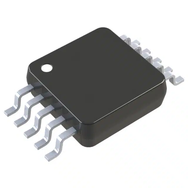
The MAX4634EUB+T comes in a compact µMAX-10 package, which simplifies integration into space-constrained designs. The pin configuration is as follows:
-
V+: Connects to the power supply (1.8V to 5.5V).
-
GND: Ground connection for stable operation.
-
IN: Control input for selecting the active switch.
-
COM: Common terminal for the SPDT switch.
-
NO: Normally open terminal.
-
NC: Normally closed terminal.
The remaining pins are reserved for additional functionality or unused in typical configurations. The straightforward pin layout ensures easy integration into circuits, even for beginners.
Electrical Characteristics for Low-Voltage Applications
The MAX4634EUB+T operates efficiently in low-voltage environments, making it suitable for battery-powered devices and portable systems. Its electrical characteristics include:
|
Feature |
Specification |
|---|---|
|
Voltage – Supply, Single (V+) |
1.8V ~ 5.5V |
|
On-State Resistance (Max) |
4Ω |
|
Current – Leakage (IS(off)) (Max) |
100pA |
|
Channel-to-Channel Matching (ΔRon) |
100mΩ |
|
Crosstalk |
-78dB @ 1MHz |
|
Charge Injection |
2pC |
|
Operating Temperature |
-40°C ~ 85°C (TA) |
The device’s low leakage current and high channel-to-channel matching ensure signal integrity in sensitive applications. Its wide operating temperature range supports reliable performance in diverse environments.
Tip: The MAX4634EUB+T’s low charge injection (2pC) reduces signal distortion during switching, making it ideal for sample-and-hold circuits and relay replacements.
Integrating the MAX4634EUB+T into Low-Voltage Circuits
Circuit Integration Basics
Integrating the MAX4634EUB+T into a low-voltage circuit requires careful planning to ensure optimal performance. The device’s compact µMAX-10 package simplifies its inclusion in space-constrained designs. Designers must first identify the appropriate location for the multiplexer within the circuit. This placement depends on the intended application, such as signal routing or data acquisition.
The control input (IN) determines the active switch state, allowing the device to toggle between the normally open (NO) and normally closed (NC) terminals. Proper configuration of this input ensures accurate signal routing. Additionally, the common terminal (COM) serves as the shared connection point for the selected signal path.
Accurate circuit integration strategies are essential for achieving reliable operation. Industries like telecommunications and consumer electronics face cost pressures, making efficient designs critical. Regulatory standards, such as the EU’s Ecodesign Directive, also emphasize energy efficiency, further highlighting the importance of precise integration. Technological advancements, including FinFET and FD-SOI technologies, demonstrate the need for accurate circuit design to maximize performance.
Power Supply and Signal Connections
The MAX4634EUB+T operates on a single supply voltage ranging from 1.8V to 5.5V. Designers must connect the V+ pin to a stable power source within this range. The GND pin should be connected to the circuit’s ground to ensure proper operation. These connections provide the foundation for the device’s functionality.
Signal connections require equal attention. The IN pin controls the switching state and should be driven by a microcontroller or logic circuit. The COM pin acts as the shared terminal for the selected signal path, while the NO and NC pins correspond to the two possible signal routes. Proper routing of these signals minimizes interference and ensures signal integrity.
The device’s low on-resistance and rail-to-rail signal handling make it suitable for a wide range of analog signals. Its low charge injection reduces distortion during switching, which is particularly beneficial in sensitive applications like sample-and-hold circuits.
Example Applications in Low-Voltage Systems
The MAX4634EUB+T finds use in various low-voltage systems due to its versatility and performance. Common applications include:
-
Audio and video signal routing, where the device switches between different input sources.
-
Battery-powered equipment, where its low power consumption extends battery life.
-
Communications circuits, where it routes RF or baseband signals efficiently.
-
Low-voltage data acquisition systems, where it switches between multiple analog inputs.
-
Sample-and-hold circuits, where its low charge injection ensures accurate signal capture.
|
Application Type |
|---|
|
Audio/Video Signal Routing |
|
Battery-Powered Equipment |
|
Communications Circuits |
|
Low-Voltage Data-Acquisition Systems |
|
Sample-and-Hold Circuits |
These examples demonstrate the device’s adaptability across various industries. Its ability to handle rail-to-rail signals and operate efficiently in low-voltage environments makes it a valuable component in modern electronic systems.
Practical Example: Using the MAX4634EUB+T with a Microcontroller
Example Circuit Diagram
The MAX4634EUB+T can be easily integrated with a microcontroller for precise signal routing. Below is a simple circuit diagram illustrating its connection:
-
V+ Pin: Connects to a 3.3V power supply.
-
GND Pin: Links to the ground of the microcontroller.
-
IN Pin: Receives a digital control signal from the microcontroller to toggle between the NO and NC terminals.
-
COM Pin: Acts as the shared terminal for the selected signal path.
-
NO and NC Pins: Connect to two different input signals.
This setup allows the microcontroller to control the signal path dynamically, making it ideal for applications like sensor switching or data acquisition.
Code Snippet for Controlling the Multiplexer
The following code demonstrates how to control the MAX4634EUB+T using an Arduino microcontroller:
#define CONTROL_PIN 7 // Define the pin connected to the IN pin of the multiplexer

void setup() {
  pinMode(CONTROL_PIN, OUTPUT); // Set the control pin as an output
}

void loop() {
  digitalWrite(CONTROL_PIN, HIGH); // Switch to the NO terminal
  delay(1000); // Wait for 1 second
  digitalWrite(CONTROL_PIN, LOW); // Switch to the NC terminal
  delay(1000); // Wait for 1 second
}
This code toggles the multiplexer between the NO and NC terminals every second, demonstrating its basic functionality.
Explanation of the Example Application
In this example, the microcontroller sends a digital signal to the IN pin of the MAX4634EUB+T. A HIGH signal selects the NO terminal, while a LOW signal selects the NC terminal. This configuration enables the microcontroller to route signals dynamically, making it suitable for applications like switching between sensors or audio sources.
Performance measurements validate the effectiveness of this setup. The impedance accuracy in a multiplexed configuration remains within 1% up to 500 kHz. Minor errors arise from cable length and phase shifts in the amplification stage. At higher frequencies, parasitic inductance slightly affects impedance and phase. Despite these factors, the MAX4634EUB+T ensures reliable performance in low-voltage circuits.
Key Considerations for Using the MAX4634EUB+T
Voltage and Current Limits
Understanding the voltage and current limits of the MAX4634EUB+T is essential for reliable operation. This multiplexer supports a supply voltage range of +1.8V to +5.5V, making it ideal for low-voltage applications. Its on-resistance (RON) varies with the supply voltage, reaching a maximum of 4Ω at +5V and 5.5Ω at +3V. These values ensure minimal signal loss across different voltage conditions. Additionally, the device exhibits an off-leakage current of only 0.1nA at +25°C, which is particularly advantageous for low-power systems.
To avoid damage, designers should ensure the supply voltage remains within the specified range. Exceeding these limits may compromise the device’s performance or lead to permanent failure. Similarly, the current through the switch should not exceed the recommended levels to maintain signal integrity and prevent overheating.
Ensuring Signal Integrity
Maintaining signal integrity is crucial when using the MAX4634EUB+T in sensitive applications. The device’s low on-resistance and high channel-to-channel matching (ΔRON of 0.2Ω max) minimize signal distortion. Its low charge injection of 2pC further reduces transient errors during switching, making it suitable for precision circuits like sample-and-hold systems.
To enhance performance, designers should use short, well-shielded signal paths to reduce noise and crosstalk. Proper grounding is also essential to prevent interference. The multiplexer’s high off-isolation (-65dB at 1MHz) and low crosstalk (-67dB at 1MHz) ensure clean signal routing, even in high-frequency applications.
Managing Power Dissipation and Thermal Performance
Efficient power management is vital for ensuring the longevity of the MAX4634EUB+T. The device consumes minimal power, making it suitable for battery-operated systems. Its power consumption scales with usage, allowing it to operate efficiently across different throughput rates. For instance, similar devices consume only 50nA in standby mode, which aids in thermal management and extends battery life.
To manage heat dissipation, designers should ensure adequate ventilation or use heat sinks in high-power applications. Operating the device within its specified temperature range (-40°C to +85°C) prevents thermal stress and ensures consistent performance.
Tip: Incorporating an automatic power-down mode can further reduce power consumption and improve thermal efficiency in portable systems.
Troubleshooting the MAX4634EUB+T in Low-Voltage Circuits
Diagnosing Signal Switching Issues
Signal switching issues often arise due to improper control input or unstable power supply connections. To diagnose these problems, verify the control signal driving the IN pin. Ensure the microcontroller outputs a clean digital signal with sufficient voltage levels to toggle the switch. Check the connections to the NO, NC, and COM pins for continuity and proper routing.
Unstable switching may result from noise or interference in the control signal. Using a pull-up or pull-down resistor on the IN pin can stabilize the signal. Additionally, inspect the PCB layout for potential crosstalk between signal traces. Shorter traces and proper shielding reduce interference and improve switching reliability.
Tip: If switching delays occur, confirm the timing requirements of the application align with the MAX4634EUB+T’s fast turn-on and turn-off times.
Resolving Power Supply Problems
Power supply issues can disrupt the operation of the MAX4634EUB+T. Begin by verifying the voltage at the V+ pin. Ensure it falls within the specified range of 1.8V to 5.5V. Check for fluctuations or noise in the supply voltage using an oscilloscope. A stable power source is essential for consistent performance.
If the device fails to operate, inspect the ground connection at the GND pin. Poor grounding can lead to erratic behavior. Adding decoupling capacitors near the V+ pin helps filter out noise and stabilize the supply voltage. For battery-powered systems, ensure the battery provides sufficient current to meet the device’s requirements.
Note: Using a regulated power supply minimizes voltage variations and ensures reliable operation in low-voltage circuits.
Addressing Signal Distortion or Noise
Signal distortion or noise can compromise the performance of the MAX4634EUB+T. To address these issues, implement RC filters to eliminate unwanted signals and reduce settling time. High-speed amplifiers, such as the ADA4899-1, provide ultralow noise and distortion, ensuring signal integrity.
Careful PCB layout plays a critical role in minimizing crosstalk and settling time. Short signal paths and proper grounding reduce interference. For applications requiring precise signal routing, use a low-output-impedance buffer to manage kickback from multiplexer inputs. Select filter capacitance carefully to balance stability and attenuation of kickback.
-
Implement a low-output-impedance buffer to manage kickback.
-
Select appropriate filter capacitance for stability and attenuation.
-
Use high-speed amplifiers with sufficient bandwidth and low noise characteristics.
These measures ensure clean signal routing and reliable operation in sensitive applications.
The MAX4634EUB+T stands out as a reliable and efficient solution for low-voltage circuits. Its low on-resistance, fast switching, and rail-to-rail signal handling make it ideal for applications like data acquisition and signal routing. Engineers and hobbyists can explore its potential in various projects, from audio systems to portable devices. Following best practices, such as proper grounding and stable power supply connections, ensures optimal performance. Experimenting with this versatile multiplexer can unlock innovative possibilities in modern electronics.
What is the primary function of the MAX4634EUB+T multiplexer?
The MAX4634EUB+T is a single SPDT analog switch. It routes signals between two paths (NO and NC terminals) based on a control input. This makes it ideal for applications like signal routing, data acquisition, and sensor switching in low-voltage circuits.
Can the MAX4634EUB+T handle rail-to-rail signals?
Yes, the MAX4634EUB+T supports rail-to-rail signal handling. This feature allows it to process signals that span the full voltage range of the power supply, ensuring compatibility with a wide variety of analog signals.
How does the control input (IN pin) work?
The IN pin determines the active signal path. A HIGH signal connects the COM pin to the NO terminal, while a LOW signal connects it to the NC terminal. This simple logic enables precise control of signal routing.
Tip: Use a microcontroller to automate the control input for dynamic switching.
What is the recommended power supply range for the MAX4634EUB+T?
The MAX4634EUB+T operates on a single supply voltage ranging from +1.8V to +5.5V. This range makes it suitable for low-voltage and battery-powered systems.
How can designers ensure signal integrity when using the MAX4634EUB+T?
Designers should use short, shielded signal paths and proper grounding. The device’s low on-resistance and high off-isolation minimize distortion and noise. Adding RC filters can further enhance signal quality in sensitive applications.
Note: Proper PCB layout plays a critical role in maintaining signal integrity.
See Also
Three Effective Methods for Integrating MC9S12XET512VAG
Understanding MC9S12DJ256MFUE Specs for Automotive Use
Unveiling LPQ252-CEF for Optimal Power Management Solutions
Ways EP2C50F484I8N FPGA Can Revolutionize Your Projects
Simple Networking Tips for XILINX XC7K325T-2FFG676C