MOSFETs, or metal-oxide-semiconductor field-effect transistors, are voltage-controlled devices. They are indispensable components in modern electronics. These transistors offer unique characteristics. A key advantage of a MOSFET’s design includes high input impedance. MOSFETs also provide fast switching capabilities and low on-resistance. This versatility makes the mosfet crucial for many applications and various circuits. These features lead to efficient power circuits. This post will detail these mosfet advantages. It will show their real-world significance for fast, low-power operation in circuit design.
Key Takeaways
-
MOSFETs are voltage-controlled devices. They need only a small voltage to work. This makes them different from older parts that need current.
-
MOSFETs have high input impedance. This means they use very little power to control. This helps make circuits simpler and more efficient.
-
MOSFETs switch on and off very fast. This helps devices like power supplies work better. It also saves energy.
-
MOSFETs have low on-resistance. This means they lose less power as heat. This makes devices run cooler and last longer.
-
MOSFETs are used in many devices. These include phones, cars, and computers. They help make these devices smaller and more powerful.
MOSFET Fundamentals: The Source of Power
MOSFET Operation Overview
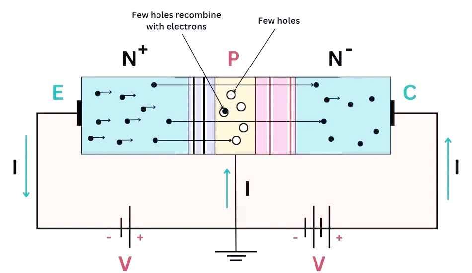
A MOSFET operates as a voltage-controlled device. A small potential applied to its gate controls the flow between its source and drain. This differs significantly from Bipolar Junction Transistors (BJTs). BJTs are current-controlled devices. They require a small input signal at the base to manage a larger flow. The working principle of a mosfet relies on an electric field. This field forms when a potential is applied to the gate. It creates a conductive channel. This channel allows charge to pass. This control makes MOSFETs very efficient in many circuits.
Key Characteristics vs. BJTs
MOSFETs possess key characteristics that set them apart. Their gate is electrically insulated by a thin oxide layer. This insulation means virtually no charge flows into the gate itself. This gives MOSFETs a high input impedance. They also offer greater flexibility. They can operate in both enhancement and depletion modes. This provides designers more options.
Consider the fundamental difference between these transistor types. A Bipolar Junction Transistor (BJT) operates by using a small input signal at the base. This input controls a much larger flow between the collector and emitter. This makes the BJT a current-controlled device. The base input directly influences the collector output. When a small forward potential is applied, electrons are injected. This creates a strong collector flow.
In contrast, a Metal-Oxide-Semiconductor Field-Effect Transistor (MOSFET) is a voltage-controlled switch. A MOSFET requires only a potential at the gate. This potential controls the flow between the source and drain. The gate is electrically insulated from the channel. This insulation means virtually no charge flows into the gate. When a positive potential is applied to the gate, it creates an electric field. This field attracts electrons. It forms a conductive channel. This allows charge to flow. This insulation gives MOSFETs high input impedance. It also contributes to low power consumption. This makes the mosfet a superior choice for many modern circuits.
Here is a comparison:
|
Property |
Bipolar Junction Transistor (BJT) |
Metal Oxide Semiconductor Field Effect Transistor (MOSFET) |
|---|---|---|
|
Control Method |
Current-controlled device |
Voltage-controlled device |
|
Input Requirement |
Small input current at the base |
Voltage at the gate |
|
Gate Insulation |
Not applicable |
Electrically insulated by a thin oxide layer |
|
Input Impedance |
Lower |
High |
This table highlights the advantages of the mosfet. It shows how it surpasses older technologies like bipolar power transistors.
Core MOSFET Advantages in Circuit Design
High Input Impedance: Simplified Design
High input impedance is a significant advantage of a mosfet’s design. Modern MOSFETs typically exhibit a high input impedance, ranging from megaohms to gigaohms. This characteristic means almost no input current is required to control the device. This simplifies driver circuits. It also reduces power consumption. Designers can achieve signal amplification without loading the source. This makes the mosfet ideal for sensitive signal processing circuits.
Fast Switching: High-Frequency Efficiency
MOSFETs offer rapid switching capabilities. This enables high-frequency operation. It also allows efficient power conversion, especially for digital signals. Switched-mode power supplies (SMPS) achieve higher efficiency than linear power supplies. Their switching transistors operate in low-dissipation, full-on and full-off states. This minimizes wasted energy. They spend very little time in high-dissipation transitions. Voltage regulation is managed by adjusting the ratio of on-to-off time (duty cycle). This method significantly improves electrical efficiency. Linear power supplies continuously dissipate power in the pass transistor. In quasi-resonant zero-current/zero-voltage switch (ZCS/ZVS) operation, each switching cycle delivers a quantized energy packet to the converter output. The switch turns on and off at zero current and voltage. This results in an ‘essentially lossless switch.’ This directly contributes to the efficiency of the power supply. This fast switching ability is a key advantage of a mosfet’s design.
Low On-Resistance: Reduced Power Loss
Low on-resistance (Rds(on)) is another crucial advantage of a mosfet’s design. This characteristic minimizes power dissipation. It also reduces heat generation. A lower Rds(on) figure in a transistor directly translates to reduced heat generation. Less power dissipates as heat when the transistor conducts current. This reduction in power dissipation leads to higher overall efficiency in power applications. This makes the mosfet highly efficient in power circuits.
Scalability and Miniaturization
MOSFETs facilitate compact designs. They also allow high integration density. This contributes to lower overall circuit costs. Production becomes less expensive. Research references include a 5nm-gate nanowire FinFET from 2004. FinFET scaling to 10 nm gate length was reported in 2002. A 25-nm gate-length FinFET transistor module for the 32nm node developed in 2009. Intel began commercial production of a process featuring a 32 nm feature size in late 2009. The actual channel length was even shorter than this stated feature size. Simulation results for SOI MG MOSFETs discuss a 15-nm gate length. This scalability is a significant advantage of a mosfet’s design. It allows for smaller, more powerful circuits.
Thermal Stability
MOSFETs offer superior thermal stability. This improves reliability in varying temperature conditions. MOSFETs generally exhibit superior thermal stability and rugged reliability compared to BJTs. MOSFETs are less prone to thermal runaway. BJTs can experience this condition if not properly managed. This inherent stability allows MOSFET amplifiers to operate in Pure Class A or very-high Class AB modes. BJT designs often require significant attention to thermal stability. This typically results in Class A/B operation to prevent thermal runaway. Lateral MOSFETs possess a negative temperature coefficient within their bias regions. This enables them to self-regulate and protect themselves at elevated operating temperatures. Conversely, Vertical MOSFETs, similar to BJTs, can be susceptible to thermal runaway if not carefully controlled. This thermal stability is a key advantage of a mosfet’s design. It ensures consistent performance in many circuits. This makes the mosfet a reliable choice for demanding applications.
MOSFET Application Circuits: Where They Shine
MOSFETs have become fundamental building blocks across a vast array of electronic systems. Their unique advantages make them ideal for many specialized applications. These mosfet application circuits demonstrate the versatility and efficiency of MOSFET technology.
Power Electronics
MOSFETs are indispensable in power electronics. They play a critical role in Switched-Mode Power Supplies (SMPS), motor control systems, and inverters. In SMPS, MOSFETs enable efficient dc-dc converters by rapidly switching current. This minimizes energy loss. For motor control, MOSFETs manage current flow to and from the motor. They safeguard against hazardous conditions. They also disconnect the motor during overcurrent or overheating events. This prevents damage. MOSFETs efficiently adjust motor speed within Pulse Width Modulation (PWM) circuits. This enhances thermal dissipation by regulating power flow and minimizing heat accumulation.
Designers often use silicon carbide (SiC) technology to enhance efficiency in high-frequency motor applications. SiC delivers higher electron mobility, lower intrinsic carrier concentration, and higher thermal conductivity. SiC MOSFETs offer higher current densities, lower switching losses, and high-temperature operation. They also operate at higher frequencies. This results in more efficient operation, less cooling, and smaller passive components. All these factors lead to a more compact solution. These advancements make MOSFETs crucial for modern power management circuits and various power converters.
Digital Circuits
MOSFETs form the backbone of modern digital circuits. They are the fundamental components for constructing CMOS logic gates. These gates are essential for microprocessors and memory. NMOS transistors activate with a ‘1’ input. PMOS transistors activate with a ‘0’ input. CMOS logic gates combine NMOS and PMOS transistors in series between the power supply and ground. This complementary arrangement prevents unnecessary current flow. It leads to low power consumption. This is why CMOS is the predominant technology in computer circuits.
RF and Communication
MOSFETs are vital in RF and communication systems. They function as amplifiers and switches in wireless devices. LDMOS (Laterally Diffused Metal Oxide Semiconductor) transistors became the standard technology for RF power amplifiers by the 1990s. They replaced bipolar junction transistors due to their superior RF performance. RF MOSFETs are specialized transistors optimized for high-frequency applications like cellular base stations. They operate efficiently at radio frequencies, from hundreds of megahertz to several gigahertz. They function as electronic switches or amplifiers. Their design includes modifications, such as specialized materials and techniques. These reduce parasitic capacitance and improve gain. These are critical for high-frequency performance in telecommunications.
The RF signal enters via the gate terminal. The gate voltage controls electron flow between the drain and source, modulating the signal. Applying voltage to the gate creates an electric field. This field influences channel conductivity. It enables amplification of the incoming RF signal. The transistor boosts the RF signal’s power from drain to source with minimal distortion. This ensures high gain at desired frequencies. The amplified RF signal exits through the drain, ready for transmission or further processing. RF MOSFETs can manage high power levels. This is essential for long-distance signal transmission without degradation. Integrated heat dissipation mechanisms prevent overheating during high-power operation. This ensures stability and longevity. RF MOSFETs are crucial in cellular base stations for enabling high-speed 4G and 5G connectivity. They amplify signals to reach distant devices. This ensures clear voice calls and rapid data transfer. Telecom providers utilize RF MOSFETs to enhance network coverage and capacity.
Automotive Electronics
MOSFETs are integral to automotive electronics. They appear in engine control units and electric vehicle power management systems. For conventional internal combustion engine vehicles, MOSFETs control components such as fuel injectors, ignition coils, and exhaust gas recirculation (EGR) valves. Their rapid switching capabilities improve engine performance. This leads to better fuel efficiency and reduced emissions. Automotive power MOSFETs offer effective switching speeds ranging from tens to hundreds of nanoseconds. This is crucial for fast response in power-intensive applications. Small signal MOSFETs can switch in just a few nanoseconds. This provides even faster response for high-speed signal processing. Lower on-state resistance (typically 10 mΩ to sub <1mΩ) increases efficiency by reducing power losses. This minimizes heat generation and energy wastage.
In electric vehicles, MOSFETs are critical for battery management systems. Split-gate trench (SGT) technology offers higher efficiency. Low on-resistance minimizes power loss. Low gate-drain charge allows faster switching. These devices operate at junction temperatures up to 175°C for reliability. Compact and powerful TOLL-8L packages offer high power density for design flexibility. MOSFETs also enable efficient dc-dc converters and other power management circuits in electric vehicles. They are also used in reverse polarity protection circuits. This protects sensitive components from incorrect power connections.
Consumer Electronics
MOSFETs enable compact and efficient power delivery in consumer electronics like smartphones, laptops, and LED lighting. Trench LV MOSFET technology, combined with low Rds(on) and low threshold voltage, significantly reduces conduction and switching losses. This reduction in losses directly enhances overall system efficiency and thermal performance. Devices like the BSS138KV integrate two independent 60V N-channel MOSFETs with ESD protection into an ultra-miniature SOT-563 package. This drastically cuts down component count and PCB footprint. The dual configuration simplifies critical functions such as load switching, level shifting circuits, and signal routing. This allows for optimized circuit architecture in multi-voltage domain applications.
Power MOSFETs integrate into smartphones and laptops to achieve efficient power regulation. Their compact size and high efficiency are crucial for enabling smaller device designs and extending battery life. Fast-charging technologies in smartphones rely on MOSFETs to safely deliver high currents. ROHM’s AW2K21 integrates two MOSFETs into a single 2.0mm x 2.0mm WLCSP package. This addresses the need for bidirectional protection and high-current handling in compact devices. This integration significantly reduces the board space required and minimizes power loss. It overcomes limitations of traditional solutions that use two larger MOSFETs. Compared to standard 3.3mm x 3.3mm MOSFETs, the AW2K21 reduces footprint by approximately 81% and ON-resistance by about 33%. It also offers up to 50% lower ON-resistance than similarly sized GaN HEMTs. These mosfet-based designs are essential for modern portable devices, including those requiring voltage level shifting and efficient switching circuits.
MOSFET Design Considerations
Gate Drive Requirements
Proper gate drive is crucial for MOSFET performance. The gate driver circuit must provide the correct turn-on and turn-off voltage for optimal device operation. It also needs sufficient peak and continuous current. This efficiently charges and discharges the gate capacitance. Gate charge (Qg) is a key factor. It determines the power requirements for the gate drive power supply. Qg also affects the average power dissipated by the gate drive resistor. A higher Qg necessitates a more robust power supply. Designers must place all gate drive components close to the main device’s gate. This reduces parasitic inductance.
Thermal Management
Effective thermal management ensures MOSFET reliability. Passive cooling methods use heat sinks and thermal pads. Active cooling systems employ fans or liquid setups. Dual-side cooling (DSC) technology is very effective. It features thermal pads on both top and bottom surfaces. This reduces thermal resistance. For high-power applications, engineers often use forced air cooling with powerful fans. This ensures efficiency and reliability in demanding operational environments. These methods protect the circuits from overheating.
Parasitic Effects
Parasitic elements within MOSFETs significantly affect performance. Gate-source capacitance (Cgs) and gate-drain capacitance (Cgd) are primary parasitic capacitances. They form the input capacitance (Ciss). These capacitances must charge and discharge for the MOSFET to switch states. This directly impacts switching speed. The Miller effect, caused by Cgd, amplifies effective gate capacitance. This increases switching time. Parasitic inductance in MOSFET packages also causes issues. High dV/dt and di/dt transients lead to spikes. These spikes can damage the device. They can also cause unintended turn-on in sensitive circuits.
Selection Criteria
Selecting the right MOSFET involves several factors. Engineers consider the application’s specific needs. They look at the required switching speed and frequency. Protection features like Under-Voltage Lockout (UVLO) are important. Input signal compatibility and power supply requirements also matter. The overall design of the power circuit depends on these choices. Cost and availability are also practical considerations for all circuits.
MOSFETs offer significant advantages. These include high input impedance, fast switching, low on-resistance, scalability, thermal stability, and versatility. These characteristics have fundamentally transformed circuit design. They enable more efficient, compact, and high-performance electronic systems. This impacts various applications, from power electronics to digital circuits. MOSFET technology remains crucial. It will continue to drive innovation across diverse industries. 🚀
FAQ
What is the main difference between a MOSFET and a BJT?
MOSFETs are voltage-controlled devices. BJTs are current-controlled devices. A MOSFET’s gate is insulated. This gives it high input impedance. A BJT requires input current at its base.
Why do MOSFETs have high input impedance?
A thin oxide layer insulates the MOSFET’s gate. This insulation prevents current flow into the gate. This characteristic means the device requires almost no input current to operate. This simplifies circuit design.
How do MOSFETs contribute to energy efficiency?
MOSFETs have low on-resistance. This minimizes power dissipation as heat. They also switch quickly. This allows for efficient power conversion in applications like switched-mode power supplies.
Where are MOSFETs commonly used?
MOSFETs are widely used in power electronics, such as SMPS and motor control. They are also fundamental in digital circuits like microprocessors. Additionally, they appear in RF communication and automotive electronics.
What is “thermal stability” in MOSFETs?
Thermal stability means a MOSFET performs reliably across varying temperatures. MOSFETs are less prone to thermal runaway than BJTs. This allows them to operate consistently, especially in high-power applications.
See Also
IRF820 N-Channel MOSFET: Powering Management, DC-DC, And Motor Control Applications
Unveiling FREESCALE MCF5251CVM140: Essential Features For Automotive System Performance
EP2C50F484I8N FPGA: Bridging Theory To Practical High-Performance Embedded System Design
Achieving Excellence In Electronic Components: Innovation, Quality, And Future Trends Explored
NXP Microcontrollers: Core Power In Automotive Electronics With Practical Applications