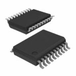
The S25FL256SAGMFI plays a vital role in improving IoT device performance by offering fast, reliable storage for firmware and critical data. Its versatility makes it suitable for applications in smart home devices, industrial sensors, and medical equipment. Developers favor this flash memory IC for its high-speed operation, low power consumption, and robust design. Key specifications include a 256M memory size, SPI interface, and a wide operating temperature range, as shown below:
|
Attribute |
Value |
|---|---|
|
Manufacturer |
|
|
Memory Size |
256M (32M x 8) |
|
Memory Type |
FLASH – NOR |
|
Speed |
133MHz |
|
Voltage Supply Range |
2.7 V ~ 3.6 V |
|
Operating Temperature Range |
-40°C ~ +85°C |
|
Interface |
SPI Serial |
|
Package Case |
SO-16 |
These features ensure seamless integration into IoT systems, even in demanding environments.
Key Takeaways
-
The S25FL256SAGMFI has 256M of fast and steady storage. It works well for IoT devices needing quick data access.
-
It uses little power, saving energy and helping batteries last longer.
-
The SPI interface makes communication easy and keeps data transfer fast.
-
It works in very hot or cold places (-40°C to +85°C), so it’s good for outdoor and industrial use.
-
Memory partitioning and error correction keep data safe and help with smooth updates.
Understanding the S25FL256SAGMFI Flash Memory IC
Key Features of the S25FL256SAGMFI
High storage capacity and fast performance
The S25FL256SAGMFI offers a memory density of 256 Mbit, making it ideal for applications requiring substantial storage. Its fast SPI speed of 133 MHz ensures quick data access, which is essential for IoT devices that demand real-time performance. This combination of high capacity and speed supports tasks like code shadowing, execute-in-place (XIP), and data storage, enabling seamless operation in embedded systems.
|
Feature |
Description |
|---|---|
|
Memory Density |
256 Mbit |
|
Voltage |
3.0 Volt |
|
Process Technology |
65nm |
|
SPI Speed |
133 MHz |
|
Multi I/O Bus |
Yes |
|
Applications |
Ideal for code shadowing, XIP, and data storage |
Low power consumption for energy-efficient IoT devices
The S25FL256SAGMFI is designed with energy efficiency in mind. Its low power requirements, operating within a voltage range of 2.7 V to 3.6 V, make it suitable for battery-powered IoT devices. This feature helps extend device lifespan while maintaining reliable performance, which is critical for applications like smart sensors and wearables.
SPI interface for seamless communication
The SPI interface simplifies communication between the S25FL256SAGMFI and microcontrollers. By reducing the number of signals required, the SPI interface minimizes design complexity while maintaining high-speed data transfer. This feature ensures compatibility with a wide range of IoT devices, from consumer electronics to industrial equipment.
Benefits for IoT Applications
Reliable storage for firmware and critical data
The S25FL256SAGMFI provides dependable storage for firmware, boot code, and critical data. Its high-density performance supports various embedded applications, ensuring IoT devices operate smoothly. For example, it enables fast firmware updates and secure data storage in smart home devices and industrial sensors.
|
Feature |
Benefit |
|---|---|
|
High-density performance |
Supports various embedded applications, including IoT. |
|
Flexibility and speed |
Ideal for code shadowing, XIP, and data storage in IoT devices. |
|
Reduced signal count |
Matches traditional parallel interface speeds while minimizing complexity. |
Compact design for space-constrained devices
The compact design of the S25FL256SAGMFI allows it to deliver high-density performance while reducing the number of signals required for operation. This efficiency is particularly valuable for IoT devices with limited physical space, such as wearables and medical instruments. By optimizing space usage, the IC ensures effective data transfer and storage without compromising functionality.
Durability for industrial and harsh environments
The S25FL256SAGMFI is built to withstand demanding conditions. Its wide operating temperature range of -40°C to +85°C ensures reliable performance in industrial and outdoor IoT applications. This durability makes it a trusted choice for devices like industrial robots and environmental sensors, where consistent operation is critical.
Setting Up the S25FL256SAGMFI in IoT Devices
SPI Interface and Communication
Overview of the SPI protocol
The Serial Peripheral Interface (SPI) protocol enables fast and efficient communication between devices. It uses a master-slave architecture, where the master device controls the communication. SPI operates with four main signals: MISO (Master In, Slave Out), MOSI (Master Out, Slave In), SCLK (Serial Clock), and CS (Chip Select). This protocol supports full-duplex data transfer, making it ideal for applications requiring high-speed communication, such as IoT systems.
Configuring SPI for optimal performance
Proper SPI configuration ensures reliable communication with the S25FL256SAGMFI. Developers should set the clock polarity (CPOL) and clock phase (CPHA) to match the IC’s requirements. The SPI clock speed should not exceed 133 MHz to maintain data integrity. Enabling pull-up resistors on unused pins can prevent signal interference. Testing the configuration with basic read/write commands verifies the setup before full implementation.
Pin Configurations and Hardware Connections
Pinout details and their functions
The S25FL256SAGMFI features 16 pins, each serving a specific purpose. Key pins include:
-
CS# (Chip Select): Activates the IC for communication.
-
SCK (Serial Clock): Synchronizes data transfer.
-
SI (Serial Input) / SO (Serial Output): Handles data input and output.
-
VCC and GND: Provide power and ground connections.
Refer to the datasheet for a complete pinout description.
Step-by-step guide to connecting the IC to a microcontroller
-
Connect the CS# pin to a GPIO pin on the microcontroller.
-
Link the SCK pin to the SPI clock pin.
-
Attach the SI and SO pins to the microcontroller’s SPI data pins.
-
Connect VCC and GND to the power supply.
-
Verify all connections using a multimeter to ensure proper continuity.
Initializing the S25FL256SAGMFI in Firmware
Required libraries and drivers
To initialize the S25FL256SAGMFI, developers need SPI libraries compatible with their microcontroller. Many platforms, such as Arduino and STM32, offer built-in SPI libraries. Additionally, the IC’s datasheet provides command sets for read, write, and erase operations.
Sample code for basic read/write operations
Below is an example of initializing the IC and performing a write operation:
#include <SPI.h>

#define CS_PIN 10  // Chip Select pin

void setup() {
  pinMode(CS_PIN, OUTPUT);
  SPI.begin();
}

void writeData(byte address, byte data) {
  digitalWrite(CS_PIN, LOW);
  SPI.transfer(0x02);  // Write command
  SPI.transfer(address);
  SPI.transfer(data);
  digitalWrite(CS_PIN, HIGH);
}

void loop() {
  writeData(0x00, 0xFF);  // Write 0xFF to address 0x00
}
This code demonstrates how to send data to the S25FL256SAGMFI using SPI. Developers can expand this example to include read and erase functions.
Optimizing the S25FL256SAGMFI for IoT Applications
Best Practices for Firmware Storage
Partitioning memory for efficient usage
Partitioning the memory of the S25FL256SAGMFI ensures efficient utilization. Developers can divide the memory into sections for firmware, configuration data, and logs. This approach prevents overwriting critical data during updates. For example, reserving a dedicated partition for boot code ensures the device can recover even if other sections fail. Proper partitioning also simplifies data management and enhances system reliability.
Ensuring data integrity during updates
Maintaining data integrity during firmware updates is crucial. Developers should implement techniques like checksums or cyclic redundancy checks (CRC) to verify data accuracy. Using a double-buffering method allows the system to store the new firmware in a separate partition before replacing the old one. This strategy ensures the device can revert to the previous version if the update fails, reducing downtime and preventing system crashes.
Data Logging and Retrieval
Techniques for fast and reliable data access
Efficient data logging and retrieval improve the performance of IoT devices. Organizing data in sequential blocks minimizes access time. Developers can use indexing to quickly locate specific data points. Implementing a circular buffer for logs ensures continuous data storage without exceeding memory limits. These techniques optimize the S25FL256SAGMFI for real-time applications like sensor data collection.
Managing wear leveling to extend IC lifespan
Wear leveling is essential for prolonging the lifespan of flash memory. The S25FL256SAGMFI benefits from algorithms that evenly distribute write and erase cycles across memory cells. Developers can implement software-based wear leveling or use built-in features of the IC. Regularly monitoring memory usage helps identify heavily used areas, allowing adjustments to prevent premature wear.
Power Management Strategies
Reducing power consumption during idle states
Reducing power consumption during idle states enhances energy efficiency. Developers can configure the S25FL256SAGMFI to enter a deep power-down mode when not in use. This mode significantly lowers current consumption, making it ideal for battery-powered IoT devices. Activating the IC only when necessary conserves energy and extends device runtime.
Configuring low-power modes for energy efficiency
Configuring low-power modes optimizes the S25FL256SAGMFI for energy-efficient operation. Developers should adjust the IC’s operating voltage to the lowest acceptable level. Using sleep or standby modes during periods of inactivity further reduces power usage. These strategies are particularly beneficial for IoT devices deployed in remote or energy-constrained environments.
Troubleshooting Common Issues with the S25FL256SAGMFI
Resolving Communication Problems
Debugging SPI connection issues
Communication problems often arise from improper SPI connections. Developers should verify the wiring between the microcontroller and the S25FL256SAGMFI. Using a multimeter helps confirm continuity for all connections, including the CS#, SCK, SI, and SO pins. Ensuring the correct voltage levels on the power supply pins is also critical. Testing the SPI interface with basic commands, such as reading the device ID, can help identify issues early. If the device does not respond, checking the SPI clock speed and ensuring it does not exceed 133 MHz is essential.
Ensuring signal integrity and proper timing
Signal integrity plays a vital role in reliable communication. Developers should use short, shielded wires to minimize noise and interference. Placing decoupling capacitors near the IC’s power pins helps stabilize the voltage supply. Proper timing is equally important. Configuring the SPI clock polarity (CPOL) and phase (CPHA) to match the IC’s requirements ensures accurate data transfer. Oscilloscopes can be used to monitor signal waveforms and detect anomalies.
Addressing Memory Corruption
Identifying and mitigating causes of data corruption
Memory corruption can occur due to power interruptions or improper write operations. Developers should implement power-fail detection circuits to prevent incomplete writes. Avoiding frequent write operations to the same memory location reduces wear and potential corruption. Monitoring error flags during read and write operations helps identify issues early.
Implementing error correction techniques
Error correction techniques enhance data reliability. Developers can use checksums or cyclic redundancy checks (CRC) to detect and correct errors. Storing redundant copies of critical data in separate memory locations provides an additional layer of protection. These methods ensure the S25FL256SAGMFI maintains data integrity even in challenging conditions.
Handling Firmware Update Failures
Strategies for safe and reliable updates
Firmware updates require careful planning to avoid failures. Developers should use a double-buffering approach, where the new firmware is written to a separate memory partition before replacing the old version. This method allows the system to revert to the previous firmware if the update fails. Verifying the integrity of the new firmware using checksums ensures it is error-free before activation.
Recovering from incomplete or failed updates
In the event of an incomplete update, the system should have a recovery mechanism. Developers can implement a bootloader that checks the firmware’s validity during startup. If the firmware is corrupted, the bootloader can load a backup version stored in a dedicated partition. This approach minimizes downtime and ensures the device remains operational.
The S25FL256SAGMFI stands out as a reliable and efficient flash memory solution for IoT systems. Its high-density performance, flexibility, and speed make it indispensable for applications requiring fast and secure data storage. The table below highlights its key features:
|
Feature |
Description |
|---|---|
|
High-Density Performance |
Supports high-density memory applications, essential for IoT devices. |
|
Flexibility |
Offers flexibility in various embedded applications. |
|
Speed |
High-speed performance with QIO and DDR-QIO commands enhances efficiency. |
|
MirrorBit Technology |
Stores two data bits per transistor, improving memory efficiency. |
|
65nm Process Lithography |
Enhances program and erase performance significantly. |
This combination of advanced features ensures seamless operation in IoT devices, even in demanding environments. By improving performance and reliability, the S25FL256SAGMFI empowers developers to create innovative and energy-efficient solutions. Exploring its capabilities can unlock new possibilities for IoT projects.
What makes the S25FL256SAGMFI suitable for IoT devices?
The S25FL256SAGMFI offers high-speed performance, low power consumption, and reliable data storage. Its compact design and wide operating temperature range make it ideal for IoT devices in diverse environments, including industrial and consumer applications.
How does the SPI interface simplify integration?
The SPI interface reduces design complexity by using fewer signals for communication. It supports high-speed data transfer, ensuring seamless integration with microcontrollers. This feature enhances compatibility with various IoT platforms, enabling efficient device communication.
Can the S25FL256SAGMFI handle harsh environments?
Yes, the S25FL256SAGMFI operates reliably in temperatures ranging from -40°C to +85°C. Its durable design ensures consistent performance in industrial and outdoor IoT applications, such as environmental sensors and industrial robots.
What strategies improve data integrity during firmware updates?
Developers can use checksums or CRC to verify data accuracy. Double-buffering stores new firmware in a separate partition before replacing the old version. This approach ensures safe updates and allows recovery if an update fails.
How can developers extend the lifespan of the S25FL256SAGMFI?
Wear leveling evenly distributes write and erase cycles across memory cells. Developers can implement software-based wear leveling or use the IC’s built-in features. Regular monitoring of memory usage helps prevent premature wear, ensuring long-term reliability.
See Also
Three Effective Methods for Integrating MC9S12XET512VAG
Fundamental Programming Skills for MC9S12XD256 Microcontrollers
Simple Networking Instructions for XILINX XC7K325T-2FFG676C
Step-by-Step Guide to Smart Home Automation with STM32F030C8T6
Explore the Essential Automotive Features of FREESCALE MCF5251CVM140