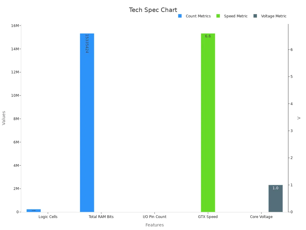
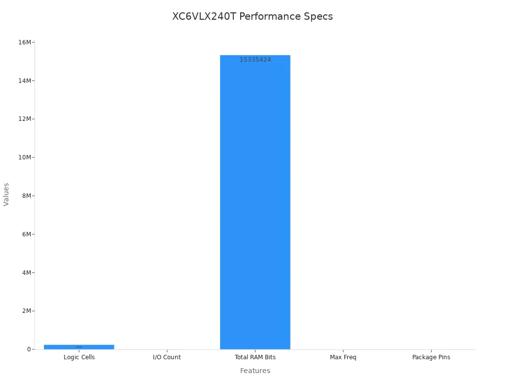
The xc6vlx240t-1ffg1759i stands out in telecommunications and defense due to its advanced virtex architecture and robust development features. Engineers rely on this fpga for telecommunications infrastructure, secure data, and mission-critical defense applications. With 241,152 logic cells, 15,335,424 RAM bits, and 720 I/O pins, this xilinx device supports a wide range of fpga applications in telecommunications development. The virtex family, including this model, ensures high-speed development and reliable operation for complex telecommunications networks and defense-grade systems.
|
Feature |
Specification/Value |
|---|---|
|
Logic Cells |
241,152 |
|
Total RAM Bits |
15,335,424 |
|
Number of I/O Pins |
720 |
|
GTX Transceiver Speed |
Up to 6.6 Gb/s |
|
PCI Express Interface |
PCIe 2.0, Gen1/Gen2, Endpoint/Root Port, x1-x8 lanes |
|
Ethernet MAC Block |
Integrated 10/100/1000 Mb/s, 2500 Mb/s support |
Key Takeaways
-
The XC6VLX240T-1FFG1759I FPGA offers high logic capacity, fast memory, and advanced I/O, making it ideal for telecom and defense systems.
-
Choosing the right FPGA means matching device features like processing power, memory, and interfaces to your project’s specific needs.
-
This FPGA supports real-time processing with low power use and strong security features, ensuring reliable and safe operation in critical environments.
-
Using evaluation kits helps engineers test FPGA performance early, reducing risks and ensuring the device meets project goals before full deployment.
-
Careful planning and cost tracking throughout development and deployment lead to successful, efficient telecom and defense applications.
Selection Criteria for FPGA
Choosing the right FPGA for telecom and defense applications requires careful evaluation of several key factors. Each project has unique development needs, so engineers must match device features to application requirements for optimal performance and cost efficiency.
Logic Resources
Logic resources form the backbone of any high-performance FPGA. Telecom and defense systems demand large numbers of logic cells to support complex processing and real-time development. Devices with advanced 6-input LUT technology increase logic density and speed, which is critical for digital signal processing and high-speed data handling.
|
Specification |
Details |
|---|---|
|
Logic Cells |
160,000 |
|
DSP Slices |
660 |
|
On-Chip Memory |
5,760 KB |
|
High-Speed Transceivers |
32 |
|
Operating Voltage |
1.0 V |
|
Temp Range |
-40°C to +100°C |
Memory and Bandwidth
High-performance telecom and defense applications require fast memory interfaces and large on-chip RAM. These features enable real-time data throughput and support advanced signal processing. FPGAs with faster memory access and high bandwidth ensure smooth operation in demanding environments.
DSP and Processing Power
Dedicated DSP blocks are essential for efficient signal processing. High-performance FPGAs excel in digital signal processing tasks, such as baseband development and radar systems. Benchmarks show that FPGAs can deliver up to 10x better processing performance and 60% less energy use compared to traditional DSPs.
I/O Interfaces
Modern telecom and defense systems rely on high-speed serial I/O, PCIe, and Ethernet interfaces. FPGAs with robust I/O support enable seamless integration with existing infrastructure and real-time communication.
Power Efficiency
Power efficiency remains a top priority in FPGA selection. Advanced design strategies like dynamic voltage scaling and clock gating help reduce power consumption. FPGAs often consume 3-10 times less power than GPUs for similar workloads, making them ideal for cost-sensitive and high-performance telecom and defense projects.
Reliability and Security
Reliability and security are non-negotiable in mission-critical environments. FPGAs use fault tolerance, redundancy, and error correction to ensure robust operation. Security features such as encryption, tamper detection, and secure key storage protect sensitive data. Adherence to industry standards and real-time monitoring further enhance system reliability.
Tip: Always align FPGA programming technology and development tools with your application’s security, reliability, and performance needs.
XC6VLX240T-1FFG1759I Features
Architecture Overview
The xc6vlx240t-1ffg1759i belongs to the virtex-6 lxt family, which represents the latest generation fpgas from xilinx. This high-performance fpga uses a flip-chip ball grid array package (FFG1759I) and supports up to 1759 pins. The device operates at voltages between 0.95 V and 1.05 V, making it suitable for both telecom and defense systems that require reliable operation in harsh environments. The architecture supports partial reconfiguration, which allows engineers to update specific sections of the fpga without interrupting the entire system. This feature proves essential for real-time development and mission-critical embedded applications.
|
Feature |
Details |
|---|---|
|
Device Family |
Virtex-6 LXT |
|
Logic Cells |
Approximately 240,000 (241,152 reported) |
|
I/O Count |
600 user I/Os |
|
Package Type |
FFG1759I (Flip-Chip Ball Grid Array) |
|
Operating Voltage |
0.95 V to 1.05 V |
|
Operating Temperature Range |
-40°C to 100°C (Junction Temperature) |
|
Total RAM Bits |
Over 15 million bits (15,335,424) |
|
Embedded IP Cores |
PCIe Gen2, Gigabit Ethernet, Multi-Gigabit Transceivers |
|
Speed Grade |
-1 (indicating performance level) |
|
Maximum Operating Frequency |
Up to 550 MHz (typical for Virtex-6) |
|
Package Pins |
1759 pins (FFG1759I) |
|
Partial Reconfiguration |
Supported |
|
Power Consumption |
Low power consumption (typical for Virtex-6) |
The architecture enables high-performance fpga boards to deliver robust development and programming capabilities for telecom and defense applications.
Logic and DSP Capabilities
The xc6vlx240t-1ffg1759i features over 240,000 logic cells and advanced 6-input LUTs, which provide the flexibility needed for complex programming and high-speed processing. Engineers use these resources to implement custom logic for digital signal processing, encryption, and protocol handling. The device includes dedicated DSP slices, which accelerate signal processing tasks such as filtering, modulation, and error correction. These capabilities make the fpga ideal for high-performance fpga boards in telecommunications infrastructure and aerospace systems.
High-performance fpga boards with this device support real-time signal processing and enable rapid development cycles. The combination of logic and DSP resources allows teams to build scalable, reliable, and secure systems for mission-critical applications.
Memory Resources
The xc6vlx240t-1ffg1759i offers more than 15 million RAM bits, supporting high-bandwidth data buffering and storage. This memory capacity ensures that high-performance fpga boards can handle real-time data streams in telecom switches, defense radar, and fpga for image and signal processing. The device supports multiple memory interfaces, which allow seamless integration with external DRAM and flash storage.
Note: Large on-chip memory resources enable real-time processing and reduce latency in high-performance fpga applications.
I/O and SERDES
This fpga provides up to 600 user I/Os and supports advanced serial transceivers (SERDES) with speeds up to 6.6 Gb/s. Engineers can implement PCIe Gen2, Gigabit Ethernet, and other high-speed protocols directly on the fpga boards. The integrated IP cores simplify development and programming, allowing rapid deployment of high-performance networking and communication solutions.
These I/O features support real-time data transfer and ensure compatibility with a wide range of telecom and defense equipment. The high I/O count and SERDES capabilities make the xc6vlx240t-1ffg1759i a top choice for high-performance fpga boards in embedded applications.
Power Optimization
The virtex-6 architecture emphasizes low power consumption without sacrificing performance. The xc6vlx240t-1ffg1759i uses dynamic voltage scaling and clock gating to minimize energy use during development and operation. These power optimization techniques help reduce heat generation and extend the lifespan of fpga boards in telecom base stations and defense platforms.
High-performance fpga boards with efficient power management support continuous real-time processing and lower operational costs. Engineers can rely on these features to meet strict energy requirements in both field and laboratory environments.
Security Features
Security remains a critical concern in telecom and defense systems. The xc6vlx240t-1ffg1759i includes advanced security features such as bitstream encryption, tamper detection, and secure key storage. These features protect sensitive data and ensure the integrity of programming and development processes.
The device supports secure boot and real-time monitoring, which help prevent unauthorized access and maintain system reliability. Engineers can use xilinx tools to implement robust security protocols, making the xc6vlx240t-1ffg1759i a trusted solution for high-performance fpga boards in mission-critical applications.
Tip: Leverage xilinx programming tools to maximize security and reliability in your high-performance fpga development.
Applications in Telecommunications and Networking
Baseband and Networking
The XC6VLX240T-1FFG1759I supports a wide range of telecommunications and networking applications. Engineers use these high-performance FPGA boards to build baseband units for cellular networks and core networking equipment. The device offers 241,152 logic cells and up to 840 user I/Os, which enable complex digital designs and extensive connectivity. Its hard IP cores, including PCIe Gen2 and Gigabit Ethernet, provide essential protocol support for telecommunications. The package ensures mechanical stability and thermal reliability, making it ideal for telecom base stations and defense-grade networking systems.
|
Feature |
Description |
|---|---|
|
Logic Cells |
241,152 logic cells enabling complex digital designs |
|
User I/Os |
720 to 840 I/Os supporting extensive connectivity |
|
Operating Speed |
Up to 550 MHz for high-speed data throughput |
|
DSP Slices |
Advanced DSP slices for efficient signal processing |
|
Hard IP Cores |
Includes PCIe Gen2, Gigabit Ethernet, and multi-gigabit transceivers critical for networking |
|
Package |
1156-pin FCBGA providing mechanical stability and thermal reliability |
|
Partial Reconfiguration |
Supports dynamic updates without full system resets |
|
Operating Temperature Range |
-40°C to 100°C ensuring reliable operation in harsh environments |
|
Total RAM Bits |
Approximately 15.3 million bits of RAM for buffering and data storage |
|
Application Suitability |
Ideal for aerospace, defense, networking, medical imaging, and baseband processing |
Signal Processing
Telecommunications applications demand high-performance signal processing. The XC6VLX240T-1FFG1759I delivers advanced DSP slices and real-time processing capabilities. Engineers achieve accurate mode decomposition for up to six modes in multimode fiber communication. The FPGA boards reach inference speeds over 100 Hz, which supports real-time telecommunications and networking tasks. Power consumption remains low at 2.4 Watts, and energy efficiency is 13 times higher than professional GPUs. Latency stays lower than GPU-based solutions, which enables closed-loop control in telecom systems. These features make the device a top choice for FPGA for image and signal processing and other high-performance applications.
|
Metric |
FPGA Performance |
Comparison / Notes |
|---|---|---|
|
Mode decomposition accuracy |
Accurate decomposition of up to 6 modes |
Demonstrates capability in multimode fiber communication |
|
Inference speed |
Over 100 Hz |
Suitable for real-time processing in telecommunications |
|
Power consumption |
2.4 Watts |
Low power usage compared to GPUs |
|
Energy efficiency |
13X higher than professional GPUs |
Significantly more energy efficient |
|
Latency |
Lower than GPUs |
Enables closed-loop control in telecom systems |
Note: High-performance FPGA boards provide the real-time processing and low latency required for modern telecommunications.
Data Throughput
High-performance FPGA boards using the XC6VLX240T-1FFG1759I excel in data throughput for telecommunications and networking. The system achieves near-ideal channel utilization of 100% at 100 Mbps Ethernet for 64-byte frames, outperforming similar FPGA applications. At 1 Gbps Ethernet, throughput reaches 721 Mbps for 64-byte frames with only 66 clock cycles of latency. The architecture supports both active and passive measurement methods, allowing precise throughput and latency calculations. Engineers can scale the design to 10 Gbps networks, which ensures future-proof telecommunications systems.
-
The FPGA boards deliver nanosecond-level latency measurements, much better than microsecond accuracy in other solutions.
-
Network performance parameters, such as throughput, latency, and packet loss, remain stable across different frame lengths and interframe gaps.
-
Compared to software-based systems, which reach only 132 Mbps at 256-byte frames and 220 Mbps at 1024-byte frames on 1 Gbps links, these FPGA boards provide much higher throughput.
These capabilities make the XC6VLX240T-1FFG1759I a leading choice for high-performance telecommunications and networking applications.
Select the Right FPGA
Define Application Needs
Selecting the right FPGA for telecom and defense applications begins with a clear understanding of project requirements. Engineers often follow a structured process based on industry standards like DO-254. This process ensures that every step in development aligns with safety and project goals. The first step involves gathering all technical and operational needs for the application. These needs may include data throughput, latency, security, and environmental conditions.
A stepwise approach helps engineers manage requirements effectively:
-
Identify the main functions the FPGA boards must perform.
-
Determine the required processing speed and data throughput.
-
Assess the amount of memory and storage needed for real-time processing.
-
Specify the number and type of I/O interfaces for connectivity.
-
Set power consumption targets to control cost and heat.
-
Define security and reliability standards for mission-critical applications.
-
Evaluate the programming and development tools required for efficient workflow.
Tip: Use performance metrics such as throughput divided by latency to quantify application needs. This formula helps compare different FPGA boards and ensures the selected device meets the required performance.
Engineers also consider advanced techniques like pipelining and parallel processing. These methods improve performance and power efficiency, which are vital for high-performance telecom and defense applications.
Match Features to Requirements
After defining application needs, engineers match these needs to the features of available FPGA boards. This step ensures that the selected device delivers the required performance, processing, and reliability. Comparative studies show that most research focuses on low-latency inference, which is critical for real-time applications like networking and signal processing.
A practical way to match features to requirements involves creating a comparison table. This table lists key performance metrics for different FPGA boards:
|
Metric |
Board A (I-GCN) |
Board B (FlowGNN) |
Board C (BoostGCN) |
|---|---|---|---|
|
Latency (ms) |
8.2 |
7.8 |
76 |
|
Throughput (Gb/s) |
30,465.1 |
26,199.6 |
1,291.1 |
Engineers use this data to select the right FPGA for their specific applications. For example, if an application requires high throughput and low latency, Board A or B would be a better choice. The design of the FPGA, such as the use of parallel processing and pipelining, directly affects these metrics.
In some cases, engineers may prioritize robustness over speed. For instance, in feature detection and matching, bypassing certain steps can increase throughput but may reduce robustness. The choice depends on the application’s goals and the required balance between speed and reliability.
Note: Matching FPGA features to application requirements ensures optimal performance, cost control, and successful deployment in telecom and defense environments.
Use Evaluation Kits
Before finalizing the selection, engineers validate their choices using evaluation kits and reference designs. These kits provide a hands-on platform for testing performance, processing, and development tools in real-world scenarios. Evaluation kits often include pre-verified reference designs, technical support, and access to advanced programming tools.
Key features of a typical evaluation kit include:
|
Feature |
Description/Specification |
|---|---|
|
FPGA Model |
Xilinx Artix 7 XC7A35/50/75/100T |
|
Memory |
256Mbit NOR FLASH, 2x 128M/256MByte DDR3 RAM |
|
ADC |
Dual channel, 12-bit resolution, 250MHz sampling rate, LVDS output |
|
DAC |
175MHz frequency, 12-bit resolution |
|
Serial Interfaces |
High-performance serial connections including SRIO (5GBaud) and PCIe 4x (Gen2) |
|
Expansion |
2x 48-pin GPIO connectors, HDMI sockets for SRIO and expansion |
|
Development Tools |
Includes design tools, IP cores, and pre-verified reference designs for telecom use cases |
|
Support |
Technical support for troubleshooting, compiling, secondary development, and long-term service |
Engineers run performance tests such as RF sweeps, noise analysis, and latency measurements. They use design examples like beamformers and channelizers to simulate real telecom and defense applications. These tests confirm that the FPGA boards meet the required performance and processing standards.
-
Performance tests include ADC noise spectral density and DAC intermodulation distortion.
-
Design examples help engineers evaluate the effectiveness of programming and development tools.
-
Technical support ensures smooth development and troubleshooting.
Engineers should always use evaluation kits to validate their FPGA selection before moving to full-scale development. This step reduces risk, controls cost, and ensures the chosen FPGA boards deliver the expected performance in real-world applications.
The XC6VLX240T-1FFG1759I stands out in telecom and defense applications. Its features support high-performance and secure applications. Engineers should always compare application needs to FPGA features. They must check if the device meets cost targets. A practical approach includes these steps:
-
List all application requirements.
-
Match features to each application.
-
Review cost for every stage.
-
Test with evaluation kits to confirm cost and performance.
-
Track cost during deployment and updates.
-
Monitor cost in maintenance.
-
Analyze cost for upgrades.
-
Compare cost with other solutions.
-
Document cost savings.
-
Report total cost at project end.
Careful planning helps engineers control cost and achieve success in demanding applications.
What makes the XC6VLX240T-1FFG1759I suitable for telecom and defense development?
Engineers choose this device for telecom and defense because it supports high-speed data, secure logic, and reliable operation. Its architecture enables rapid development and deployment on fpga boards, meeting strict requirements for mission-critical systems.
How do fpga boards help reduce overall project cost?
Fpga boards allow engineers to reprogram hardware during development. This flexibility helps teams avoid expensive redesigns. By using fpga boards, organizations can adapt to new standards and lower the total cost of ownership over time.
Can engineers use evaluation kits for fpga boards before full-scale deployment?
Yes, evaluation kits let engineers test fpga boards in real-world scenarios. These kits support development, help verify performance, and ensure the boards meet project needs. Using evaluation kits can prevent costly mistakes and speed up the development process.
Why is power efficiency important for fpga boards in telecom and defense?
Power efficiency keeps fpga boards cool and reliable. Lower power use reduces heat, which extends the life of the boards. Efficient fpga boards also lower energy cost, making them ideal for telecom and defense development.
What role does on-chip memory play in fpga boards for high-speed applications?
On-chip memory in fpga boards stores data for fast access during development. This feature supports real-time processing and high data throughput. Engineers rely on large memory resources to keep boards running smoothly in demanding telecom and defense environments.
See Also
Top Reasons To Select Coilcraft XPL2010 For VRM
Simple Networking Tips For Xilinx XC7K325T-2FFG676C
Explore Main Automotive Features Of Freescale MCF5251CVM140
Enhancing Automotive Performance Using NXP MC9S12XEP100 Series
Uncover Essential Specifications Of MC9S12XEQ512CAL Microcontroller