Designers often face challenges when building efficient power conversion systems for compact electronics. The TP86R203NL meets these needs with a small package and high current rating. Engineers use this device to create reliable TP86R203NL supply rails in modern circuits. Its low resistance and fast switching help reduce heat and power loss.
Key Takeaways
-
The TP86R203NL is a compact, high-current MOSFET ideal for efficient DC-DC converters due to its low resistance and fast switching.
-
Choose synchronous buck or boost converter topologies to maximize efficiency and reduce heat when using the TP86R203NL.
-
Use wide copper traces, thermal vias, and good airflow in PCB layout to manage heat and improve reliability.
-
Select a fast gate driver and keep traces short and wide to reduce switching losses and signal noise.
-
Test circuits carefully by checking connections, monitoring voltages and temperature, and observing switching waveforms to ensure safe and reliable operation.
TP86R203NL Overview
Key Specs
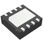
The TP86R203NL stands out as a high-performance N-Channel MOSFET. Toshiba designed this device for modern power electronics. It uses a compact 8-SOP package, which fits well in tight spaces on printed circuit boards. The device supports a drain-to-source voltage of 30 volts and can handle a continuous drain current of up to 19 amperes at 25°C. This makes it suitable for medium power switching tasks.
The table below highlights the main specifications:
|
Parameter |
Value |
|---|---|
|
Package |
8-SOP (3.90mm width) |
|
Drain-Source Voltage |
30 V |
|
Continuous Drain Current |
19 A (at 25°C) |
|
On-Resistance (Rds On) |
6.2 mΩ (at 9A, 10Vgs) |
|
Gate Threshold Voltage |
Max 2.3 V |
|
Max Gate Charge (Qg) |
17 nC (at 10V) |
|
Input Capacitance (Ciss) |
1400 pF (at 15V) |
|
Power Dissipation |
1 W (max) |
|
Operating Temp. |
Up to 150°C |
Tip: The low on-resistance helps reduce power loss and heat, which improves efficiency in DC-DC converter designs.
Application Areas
Engineers use the TP86R203NL in many power management systems. Its high current rating and fast switching make it a strong choice for several applications:
-
DC-DC Converters: The device works well in synchronous buck or boost converters. It helps lower power loss and keeps circuits cool.
-
High-Current Power Supplies: Designers use it in server power rails, telecom boards, and industrial supplies that need efficient, high-current paths.
-
Automotive and Industrial Electronics: The MOSFET’s durability and high temperature rating support automotive power distribution and embedded controllers.
-
Motor Drives and Actuators: Its speed and low switching loss make it ideal for small motor drivers and actuator circuits.
The TP86R203NL offers flexibility for engineers who need reliable and efficient switching in compact designs.
Integration Steps
Topology Selection
Engineers start by choosing the right DC-DC converter topology for their project. The TP86R203NL works well in several common designs. Buck converters step down voltage and suit applications that need lower output voltage than input. Boost converters step up voltage and help when the output must be higher than the input. Synchronous topologies use two MOSFETs instead of a diode. This approach reduces power loss and improves efficiency. The TP86R203NL performs best in synchronous buck or boost converters because of its low on-resistance and fast switching speed.
Tip: Synchronous topologies help reduce heat and increase efficiency in high-current designs.
When selecting a topology, engineers consider the input and output voltage, current requirements, and efficiency goals. For example, a server power rail often uses a synchronous buck converter to deliver stable, low-voltage, high-current power.
Schematic and Pinout
After selecting the topology, engineers move to the schematic design. The TP86R203NL comes in an 8-SOP package. Each pin has a specific function. The main pins include the drain, source, and gate. The drain connects to the load or inductor, the source connects to ground or the low side of the circuit, and the gate connects to the controller or driver.
A typical schematic places the MOSFET close to the controller. This placement helps reduce signal delay and noise. Engineers use short, wide traces for the drain and source connections. This layout reduces resistance and power loss.
Note: Always check the datasheet for the exact pinout and recommended connections.
Here is a simple pinout table for reference:
|
Pin Number |
Function |
|---|---|
|
1-3 |
Source |
|
4 |
Gate |
|
5-8 |
Drain |
Layout and Thermal
PCB layout plays a key role in the performance of any DC-DC converter. The TP86R203NL needs careful placement to handle high current and manage heat. Engineers use wide copper pours for the drain and source pins. This design lowers resistance and spreads heat across the board.
Placing thermal vias under the MOSFET helps move heat to other PCB layers. This step keeps the device cool during operation. Good airflow around the MOSFET also helps with cooling. Engineers avoid placing sensitive signal traces near the switching nodes. This practice reduces noise and improves reliability.
Alert: Poor layout can lead to overheating and power loss. Always follow best practices for thermal management.
Engineers often use simulation tools to check the thermal performance before building the board. These tools help spot hot spots and guide improvements in the layout.
Design Tips
Performance Optimization
Engineers can unlock the full potential of the TP86R203NL by focusing on a few key areas. They often select a gate driver that matches the MOSFET’s fast switching speed. A strong gate drive reduces switching losses and keeps the device cool. Short, wide traces for the drain and source lower resistance and improve current flow.
Tip: Place the MOSFET close to the controller to minimize signal delay and noise.
A low-inductance layout helps prevent voltage spikes during switching. Engineers also use high-quality ceramic capacitors near the MOSFET. These capacitors filter noise and stabilize voltage.
Checklist for Optimization:
-
Use a gate driver with fast rise/fall times
-
Keep traces short and wide
-
Add ceramic bypass capacitors close to the MOSFET
-
Simulate thermal performance before finalizing the layout
Reliability
Long-term reliability starts with proper component selection and layout. The TP86R203NL handles high current, but engineers must ensure the PCB can carry this load. Wide copper pours and thermal vias help spread heat.
Note: Always operate the MOSFET within its rated voltage and current limits.
Engineers often add extra copper thickness for high-current paths. They also check for proper soldering and avoid voids under the MOSFET. Good airflow or heatsinking extends the device’s life.
Reliability Table:
|
Factor |
Best Practice |
|---|---|
|
Current Handling |
Wide copper traces |
|
Heat Management |
Thermal vias, airflow |
|
Solder Quality |
Avoid voids, ensure coverage |
Common Pitfalls
Some mistakes can reduce performance or cause failure. Engineers sometimes overlook the importance of layout. Long, thin traces increase resistance and heat. Placing sensitive signals near switching nodes can cause noise problems.
⚠️ Alert: Never exceed the maximum voltage or current ratings.
Engineers should double-check the pinout before soldering. Incorrect connections can damage the MOSFET. They should also verify the gate drive voltage matches the device’s requirements.
Common Pitfalls List:
-
Using traces that are too narrow
-
Ignoring thermal management
-
Placing signals too close to switching nodes
-
Applying incorrect gate voltage
By following these tips, engineers can achieve efficient and reliable designs with the TP86R203NL.
Testing and Troubleshooting
Test Procedures
Engineers test the TP86R203NL,LQ in DC-DC converter circuits to confirm performance and safety. They start by checking all connections and verifying the MOSFET orientation. Power supplies should remain off during this inspection. After confirming the setup, they use a multimeter to check for shorts between the drain, source, and gate pins.
Once the circuit passes initial checks, engineers power the board with a current-limited supply. They monitor the input and output voltages. If the voltages match the design values, they proceed to measure the MOSFET’s temperature using a thermal camera or infrared thermometer. The device should stay within its rated temperature range.
Tip: Always increase the load gradually. This approach helps spot issues before they cause damage.
Engineers also use an oscilloscope to observe switching waveforms at the gate and drain. Clean, sharp transitions indicate proper operation. They record efficiency by measuring input and output power.
Basic Test Checklist:
-
Inspect solder joints and pin orientation
-
Check for shorts with a multimeter
-
Power up with current limit
-
Measure voltages and temperature
-
Observe switching waveforms
-
Record efficiency
Debugging
If the circuit does not work as expected, engineers follow a systematic approach to find the problem. They first check for visible signs like damaged components or burnt traces. Next, they verify the gate drive voltage. A low or missing gate signal can prevent the MOSFET from switching.
Engineers use the following table to guide their debugging process:
|
Symptom |
Possible Cause |
Solution |
|---|---|---|
|
No output voltage |
Gate drive issue |
Check controller and wiring |
|
Excessive heating |
Poor layout or overload |
Improve cooling, check load |
|
No switching waveform |
Faulty driver or MOSFET |
Replace driver or MOSFET |
|
Noise on output |
Layout or filtering |
Add capacitors, reroute traces |
⚡ Alert: Never touch the board while powered. High currents can cause injury.
By following these steps, engineers ensure the TP86R203NL,LQ operates safely and efficiently in their DC-DC converter designs.
TP86R203NL Example Circuit
Schematic
A typical DC-DC synchronous buck converter uses the TP86R203NL as the main switching element. The following schematic shows a basic example. In this circuit, the MOSFET controls the flow of current from the input to the output. The controller IC drives the gate. The inductor and output capacitor smooth the voltage.
Vin ----+-----+-------------------+
        |     |                   |
       [C1]  [L1]                [C2]
        |     |                   |
       GND   Drain              Output
              |                   |
           TP86R203NL           GND
           Gate <--- Driver IC
           Source --- GND
Note: Always check the datasheet for the correct pinout and recommended layout.
Component Choices
Engineers select each component to match the performance of the TP86R203NL. The input capacitor (C1) should have a low ESR to handle switching noise. The inductor (L1) must support the maximum output current and prevent saturation. The output capacitor (C2) filters voltage ripple.
A typical component selection might look like this:
|
Component |
Recommended Type |
Purpose |
|---|---|---|
|
C1 |
22µF Ceramic, Low ESR |
Input voltage filtering |
|
L1 |
4.7µH, 20A rated |
Stores energy, smooths current |
|
C2 |
47µF Ceramic, Low ESR |
Output voltage filtering |
|
Driver IC |
Fast MOSFET driver |
Controls gate switching |
-
Engineers often use ceramic capacitors for their stability.
-
The inductor rating should always exceed the maximum load current.
-
The driver IC must provide enough current for fast switching.
Tip: Proper component selection ensures stable operation and high efficiency.
Engineers can achieve efficient and reliable DC-DC converter designs by following the integration steps for the TP86R203NL. This device offers high current capability, low resistance, and a compact package. Careful layout, proper component selection, and thorough testing help maximize performance and reliability. Readers should apply these best practices in their own projects. For detailed information, always review the latest datasheet and application notes.
What is the maximum current the TP86R203NL,LQ can handle?
The TP86R203NL,LQ supports a continuous drain current of up to 19 amperes at 25°C. This rating makes it suitable for high-current applications like power supplies and motor drivers.
Can engineers use the TP86R203NL,LQ in automotive designs?
Yes, engineers can use this MOSFET in automotive systems. Its high temperature rating and MSL-1 durability support robust operation in automotive power distribution and embedded controllers.
How does the TP86R203NL,LQ improve efficiency in DC-DC converters?
The device features a low on-resistance of 6.2 mΩ and fast switching speed. These characteristics help reduce power loss and heat, which leads to higher efficiency in DC-DC converter circuits.
What layout tips help with thermal management?
Wide copper pours for the drain and source pins spread heat.
Thermal vias under the MOSFET move heat to other PCB layers.
Good airflow around the device also helps keep temperatures low.
Which gate driver works best with the TP86R203NL,LQ?
A fast MOSFET gate driver matches the TP86R203NL,LQ’s switching speed. The driver should provide enough current for quick transitions and support a gate voltage up to 10V for optimal performance.
See Also
Unlocking The Power Efficiency Of LPQ252-CEF Technology
Step-By-Step Guide To Using AEAT-8800-Q24 In Robotics
IRF820 N-Channel MOSFET Applications In Power And Motor Control
Three Best Methods To Implement MC9S12XET512VAG Effectively
In-Depth Look At MC9S12DJ256MFUE Specs For Automotive Use