The Xilinx XC7Z012S-2CLG485I stands out in automation for its seamless integration of programmable fpga logic and dual-core arm processing. This xilinx xc7z012s soc merges fpga flexibility with the power of two arm Cortex-A9 cores, giving every system high-speed control and custom hardware acceleration. Xilinx engineers designed this zynq device for demanding environments, with support for extended temperature ranges and robust connectivity like CAN, Ethernet, and USB. Users rely on xilinx fpga and arm solutions to create advanced automation projects and efficient system designs. The zynq architecture in this fpga enables precise project control across industrial and embedded system applications.
Feature
Specification
Processor
Dual arm Cortex-A9
Logic Elements
74,000 LE
Operating Range
-40°C to +100°C
Connectivity
Ethernet, USB, CAN, I2C
Key Takeaways
-
The Xilinx XC7Z012S-2CLG485I combines a dual-core ARM Cortex-A9 processor with Artix-7 FPGA logic to deliver fast and flexible system control.
-
This SoC supports many interfaces like Ethernet, USB, CAN, and I2C, making it easy to connect sensors and devices in automation projects.
-
Vivado software helps users design hardware by creating block designs and automating system setup, while Vitis supports software development and debugging.
-
Programming the FPGA with bitstream files and developing software on the ARM processor enable custom hardware acceleration and efficient system operation.
-
Testing both hardware and software thoroughly ensures reliable performance and helps catch issues early in automation system deployment.
xilinx xc7z012s soc Overview
Architecture
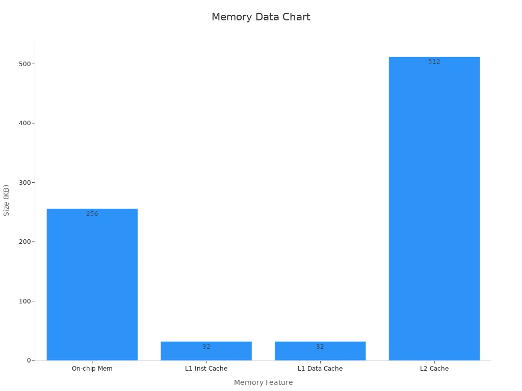
The xilinx xc7z012s soc uses a unique architecture that combines fpga logic with a powerful arm processor. This system features a dual-core ARM Cortex-A9 running at up to 766 MHz. The architecture includes 256 KB of on-chip memory, 32 KB instruction and 32 KB data L1 cache per core, and a 512 KB L2 cache. The fpga logic fabric is based on Artix-7 technology and contains 55,000 logic cells. This design allows the system to handle both software and hardware tasks efficiently. The xilinx zynq platform supports DDR3, DDR3L, DDR2, and LPDDR2 memory, making it flexible for many applications.
The integration of programmable logic and arm processing in the xilinx xc7z012s soc enables developers to create custom hardware accelerators and manage complex system tasks with ease.
|
Feature |
Specification |
|---|---|
|
Processor Type |
Dual-core ARM Cortex-A9 |
|
Processor Speed |
766 MHz |
|
On-chip Memory |
256 KB |
|
L1 Cache (per processor) |
32 KB instruction + 32 KB data |
|
L2 Cache |
512 KB |
|
Programmable Logic |
Artix-7 FPGA with 55K logic cells |
|
External Memory Support |
DDR3, DDR3L, DDR2, LPDDR2 |
|
Peripherals & Interfaces |
DMA, UART, CAN 2.0B, I2C, SPI, USB 2.0 OTG, tri-mode gigabit Ethernet |
|
Package |
485-CSBGA (19×19) |
|
Operating Temperature Range |
-40°C to 100°C (TJ) |
Key Features
The xilinx xc7z012s soc stands out for its high-speed processing and advanced fpga capabilities. The system uses an arm Cortex-A9 core that can reach up to 1 GHz and delivers 2.5 DMIPS/MHz performance. The fpga logic fabric supports hardware acceleration and digital signal processing. The system includes an 8-channel DMA controller, multiple UART, CAN, I2C, SPI, and USB 2.0 interfaces, and dual gigabit Ethernet. Security features such as RSA authentication and AES/SHA decryption protect the system during boot and operation.
|
Feature Category |
Specification / Metric |
|---|---|
|
Processor Core |
ARM Cortex-A9 single-core |
|
Maximum CPU Frequency |
Up to 1 GHz |
|
Performance |
2.5 DMIPS/MHz per CPU |
|
Cache |
32KB instruction + 32KB data L1 cache per processor; 512KB L2 cache |
|
On-chip Memory |
256KB |
|
FPGA Logic Cells |
Integrated 28nm Artix-7 based programmable logic |
|
Hardware Acceleration |
Programmable logic and DSP blocks |
|
DMA Controller |
8-channel DMA controller |
|
Communication Interfaces |
2 x UART, 2 x CAN 2.0B, 2 x I2C, 2 x SPI, 2 x USB 2.0 (OTG), 2 x tri-mode Gigabit Ethernet, 2 x SD/SDIO |
|
Memory Support |
DDR3, DDR3L, DDR2, LPDDR2, 2 x quad-SPI, NAND, NOR |
|
Security Features |
RSA authentication, AES and SHA 256-bit decryption and authentication for secure boot |
Automation Benefits
The xilinx xc7z012s soc brings many advantages to automation and industrial systems. The zynq architecture allows real-time control and fast data processing. The fpga logic fabric accelerates tasks such as signal processing and motor control. The arm processor manages system-level operations and communication. The system supports a wide range of interfaces, making it easy to connect sensors, actuators, and networks. The zynq-7000 fpga platform ensures reliable operation in harsh environments. Xilinx provides robust development tools, which help engineers design, test, and deploy automation solutions quickly. The combination of fpga flexibility and arm processing power makes the xilinx xc7z012s soc a top choice for modern automation projects.
Setup
Hardware Requirements
To begin working with the xilinx xc7z012s soc, users need the right hardware. The main component is a development board that features the AMD XC7Z012S-2CLG485I device. This board provides access to the programmable logic and the dual-core ARM Cortex-A9 processor. Users also need a reliable power supply that matches the board’s voltage and current requirements. A USB cable connects the board to a computer for programming and debugging. Many xilinx boards include Ethernet ports, SD card slots, and expansion headers for additional peripherals.
A typical hardware setup includes:
-
Xilinx Zynq-7000 development board (with XC7Z012S-2CLG485I)
-
Power supply (as specified by the board manufacturer)
-
USB cable (for JTAG and UART connections)
-
Ethernet cable (for network connectivity)
-
SD card (for booting and storage)
-
Jumper wires and headers (for custom connections)
Tip: Always check the board manual for the correct jumper settings before powering up the hardware.
Software Tools
Developers use several software tools to design, program, and debug projects on the xilinx xc7z012s soc. The main tool is vivado, which provides a complete environment for creating a project, designing the hardware, and generating the bitstream. Vivado includes features for block design, IP integration, and simulation. For software development, users can choose between the Xilinx SDK and vitis. Vitis supports both bare-metal and Linux-based applications, making it flexible for different project needs.
The essential software tools include:
|
Tool |
Purpose |
|---|---|
|
Vivado |
Hardware design, block integration, synthesis, implementation, and bitstream generation |
|
Vitis |
Software development, debugging, and deployment |
|
Xilinx SDK |
Legacy software development tool for Zynq devices |
|
Device Drivers |
Enable communication between hardware and software |
|
Serial Terminal |
Monitors UART output from the board |
Vivado guides users through creating a project, adding IP blocks, and connecting them to the processing system. The block design feature in vivado allows users to drag and drop components, making the process visual and intuitive. When users finish the design, they can use the “run block automation” and “run connection automation” features to automatically configure connections and settings. These steps help ensure the hardware design matches the requirements of the software.
Board Configuration
After gathering the hardware and installing the software, users can start configuring the board. First, connect the development board to the computer using the USB cable. Power on the board and launch vivado. Begin by creating a project in vivado, selecting the correct board and device. Use the block design editor to add the Zynq processing system and any required peripherals. Vivado provides the “run block automation” tool to set up the processing system quickly. Next, use “run connection automation” to link the processing system to memory and interfaces.
Once the block design is complete, validate the design in vivado. Generate the bitstream file, which programs the hardware. Open vitis or the xilinx SDK to create the software application. Import the hardware description from vivado and write the application code. Vitis supports C and C++ programming for both bare-metal and Linux projects.
Common setup issues include incorrect jumper settings, missing device drivers, or mismatched board selections in vivado. Users should double-check all connections and settings. If the board does not appear in vivado, try reinstalling the xilinx cable drivers or using a different USB port.
Note: Always save the vivado project frequently to avoid losing progress during hardware or software configuration.
vivado Hardware Project
Project Creation
Engineers start a vivado project by launching the vivado tool and selecting “Create New Project.” They choose a name and a location for the project. The system prompts them to select the xilinx board that contains the fpga device. After this, they move to creating a block design. This step forms the foundation for the hardware system. The block design window allows users to add and connect different system components. Vivado guides users through each step, making the process clear and organized.
Tip: Save the vivado project often to prevent data loss during design changes.
Processing System
The next step involves adding the zynq processing system to the block design. This block represents the dual-core ARM processor and its connections to the fpga logic. Users double-click the block to configure system settings such as clock frequency, memory interfaces, and boot options. Vivado provides automation tools that help set up the processing system quickly. The block connects to other system components through AXI interfaces. Engineers can adjust the hardware configuration to match the needs of their application.
A typical configuration includes:
-
Setting the clock source for the system
-
Enabling DDR memory support
-
Configuring boot options for the fpga
Peripherals Integration
After configuring the processing system, engineers add peripherals to the block design. Common peripherals include gpio, UART, SPI, and I2C. The gpio block allows the system to interact with external devices like LEDs or switches. Users drag the gpio block into the design and connect it to the processing system using AXI interfaces. Vivado makes it easy to map gpio pins to specific fpga pins. The system can support multiple gpio blocks for different functions. Engineers also add other hardware blocks as needed for their project. Vivado checks the block connections and validates the design before generating the bitstream.
Note: Always review the block diagram to ensure all system connections are correct before moving to the next step.
zynq Deployment
Bitstream Programming
Engineers use vivado to generate bitstream files for the XC7Z012S-2CLG485I device. The bitstream contains the configuration data that defines the hardware logic. After completing the hardware design, they select “generate bitstream” in vivado. The tool compiles the design and creates the bitstream file. This file allows users to program the fpga with the custom logic. To program the fpga, they connect the development board to the computer and use the hardware manager in vivado. The process involves loading the bitstream into the device memory. Many engineers choose to program the fpga at power-up by storing the bitstream on an SD card or flash memory. This method ensures the fpga loads the correct configuration every time the system starts.
Tip: Always verify the bitstream file before using it to program the fpga. This step helps prevent configuration errors.
Software Development
After programming the hardware, engineers focus on software development. They launch vitis ide to create a software project. The software runs on the ARM Cortex-A9 processor inside the Zynq device. Vitis provides templates for both bare-metal and Linux applications. Developers import the hardware description from vivado and write code in C or C++. The software can control peripherals, process data, and communicate with external devices. Vitis includes debugging tools that help engineers test and optimize their code. Many teams use vitis to build drivers and application logic for their automation projects.
Note: Good software design improves system reliability and performance.
Testing
Testing ensures the system works as expected. Engineers test both the hardware and software after they program the fpga and deploy the application. They use test scripts and serial terminals to monitor system output. The team checks if the bitstream loads correctly and if the software responds to inputs. They also verify communication with peripherals like UART, SPI, and Ethernet. If issues appear, engineers review the bitstream and software code for errors. Testing helps catch problems early and ensures the automation system meets project requirements.
Engineers recommend documenting all test results for future reference.
The AMD XC7Z012S-2CLG485I stands out in automation with its strong integration of ARM processing and Artix-7 FPGA logic. This device offers flexible design options and high performance for many applications. The table below highlights its key strengths:
|
Feature |
Details |
|---|---|
|
Processor |
ARM Cortex-A9, up to 766MHz |
|
FPGA Integration |
Artix-7, 55K logic cells |
|
Connectivity |
CAN, Ethernet, USB, I2C, SPI, GPIO |
|
Security |
RSA, AES, SHA for secure boot |
|
Application Suitability |
AI, 5G, IoT, industrial control, embedded vision |
Engineers can use this platform to build custom automation projects. Exploring its features helps users learn and innovate in embedded system design.
What makes the xilinx xc7z012s soc ideal for automation projects?
The xilinx xc7z012s soc combines fpga logic and arm processing. This integration supports fast data handling and real-time control. Many engineers choose this soc for automation because it offers flexibility and reliable performance in demanding environments.
How does vivado help with creating a project on the zynq-7000 fpga?
Vivado guides users through creating a project and building a hardware system. The tool supports creating a block design, adding the zynq processing system, and connecting peripherals. Vivado also helps generate bitstream files for programming the fpga.
What is the purpose of run block automation and run connection automation in vivado?
Run block automation sets up the zynq processing system quickly. Run connection automation links the processing system to memory and interfaces. These features save time and help ensure correct connections in the hardware design.
How do engineers program the fpga and deploy software on the system?
Engineers use vivado to generate bitstream files and program the fpga. They launch vitis ide to create a software project. The software runs on the arm processor and controls the system’s peripherals and functions.
Can users expand the system with additional gpio or peripherals?
Yes, users can add gpio blocks and other peripherals in vivado. The block design editor allows easy integration. This flexibility lets engineers customize the system for different automation needs.
See Also
A Simple Networking Tutorial For Xilinx XC7K325T Chip
In-Depth Look At MC9S12DJ256MFUE Specs For Cars
Unveiling The Main Features Of MC9S12XEQ512CAL Microcontroller
Three Best Methods To Incorporate MC9S12XET512VAG Effectively
Fundamental Programming Tips For MC9S12XD256 Microcontrollers