This article clarifies the fundamental differences between Bipolar Junction Transistors (BJTs) and Metal-Oxide-Semiconductor Field-Effect Transistors (MOSFETs). These devices are crucial components in modern electronics. Understanding their distinctions is vital for effective circuit design. A bipolar junction transistor is a current-controlled device. Conversely, a metal oxide semiconductor field effect transistor operates as a voltage-controlled device. BJTs are projected to hold 38.9% of the small signal market revenue by 2025. MOSFETs will command 30% of the power device market by 2028. This comparison of mosfet transistor, BJT will help engineers choose the right component.
Key Takeaways
-
BJTs use current to control them. MOSFETs use voltage to control them. This is the main difference between them.
-
MOSFETs switch on and off faster than BJTs. This makes MOSFETs good for quick tasks.
-
MOSFETs need very little current to work. BJTs need more current to work.
-
Engineers use BJTs for simple, low-cost jobs like making sound louder. Engineers use MOSFETs for fast, powerful jobs like in computer power supplies.
-
Choosing between a BJT and a MOSFET depends on what the electronic circuit needs to do.
BJT Transistors: Fundamentals

BJT Definition and Structure
A BJT, or bipolar junction transistor, is a three-terminal semiconductor device. It serves as a fundamental building block in electronic circuits. The three terminals are the emitter, base, and collector. Engineers use BJTs for amplification or switching electronic signals. This transistor comes in two main types: NPN and PNP. The NPN type uses electrons as its primary charge carriers. The PNP type uses holes. The internal structure of a BJT involves two PN junctions. These junctions are formed by doping semiconductor materials.
BJT Working Principle
A BJT operates as a current-controlled device. A small current flowing into the base terminal controls a much larger current between the collector and emitter. This small base current effectively “turns on” the transistor. It allows a significant current to flow through the device. Without a base current, the BJT remains in an “off” state. This control mechanism makes the BJT suitable for signal amplification. The base current dictates the collector current, providing a proportional output.
Key BJT Characteristics
One crucial characteristic of a BJT is its current gain, often denoted as beta (β) or hFE. This value indicates how much the collector current increases for a given base current. A high current gain means a small base current can control a large collector current. This feature is essential for effective amplification. For small-signal transistors, the common-emitter current gain (βF or hFE) is typically greater than 50. However, transistors designed for high-power applications may have a smaller beta value. Generally, the forward common emitter current gain (β) ranges from 20 to 500. This wide range allows for versatile signal amplification across various applications. The BJT also exhibits a relatively low input impedance. This characteristic means it requires a certain amount of current to operate the base.
MOSFET Transistors: Fundamentals
MOSFET Definition and Structure
A MOSFET, or metal oxide semiconductor field effect transistor, is a voltage-controlled semiconductor device. It forms a crucial component in modern electronics. This transistor has four terminals: the source, drain, gate, and body (or substrate). The gate terminal is insulated from the conductive channel. This insulation creates a very high input impedance. Engineers use MOSFETs widely for switching and amplification tasks. They come in two main types: enhancement mode and depletion mode. The internal structure includes a metal gate, an oxide insulator, and a semiconductor substrate.
MOSFET Working Principle
A MOSFET operates based on an electric field. The voltage applied to the gate terminal creates this field. This field controls the conductivity of a channel between the source and drain. For an N-channel mosfet, a positive voltage on the gate attracts electrons. These electrons form a conductive channel. This channel allows current to flow from the drain to the source. Conversely, a zero or negative voltage repels electrons, effectively turning the mosfet off. This voltage control mechanism makes the mosfet highly efficient for switching applications. It requires minimal gate current to operate.
Key MOSFET Characteristics
A key characteristic of a mosfet is its extremely high input impedance. The insulated gate draws almost no current. This feature simplifies the driving circuitry significantly. Another important parameter is transconductance (gm). Transconductance measures the change in drain current for a given change in gate-source voltage. It indicates the mosfet’s efficiency in converting voltage to current. Different mosfet applications require varying transconductance values:
|
MOSFET Application |
Transconductance (gm) |
|---|---|
|
Power MOSFET (Buck Converter) |
25 S |
|
Error Amplifier (Buck Converter) |
200 μA/V |
|
Current Sense (Buck Converter) |
10 mA/V |
|
Transimpedance Amplifier (TIA) |
> 20 mA/V (requirement for 1 GHz bandwidth) |
These values show the versatility of the mosfet across diverse circuit designs. The mosfet transistor offers fast switching speeds and low power dissipation in many applications. This makes it ideal for power electronics.
BJT vs MOSFET: Key Differences
Control Mechanism: Current vs. Voltage
The fundamental difference between a bipolar junction transistor and a metal oxide semiconductor field effect transistor lies in their control mechanisms. A BJT operates as a current-controlled device. A small current injected into its base terminal dictates a larger current flow between the collector and emitter. This means the BJT requires a continuous base current to maintain its “on” state. Conversely, a mosfet functions as a voltage-controlled device. The voltage applied to its gate terminal creates an electric field. This field modulates the conductivity of the channel between the source and drain. A mosfet requires virtually no gate current to maintain its state once the gate capacitance charges. This distinction profoundly impacts circuit design and power consumption.
Input Impedance and Drive Requirements
The input impedance of these two transistor types varies significantly. MOSFETs possess a significantly higher input impedance compared to BJTs. This characteristic makes mosfet easier to integrate with other circuit components. It also reduces the load on the driving circuitry. Conversely, BJTs, with their lower input impedance, may necessitate additional circuitry to manage load requirements in certain applications.
-
BJTs: Low input impedance
-
MOSFETs: Very high input impedance
For example, if a 1mV step change is applied to the base of a BJT and the input current rises by 2uA, the input resistance (h_ie) calculates to 500Ω (1mV / 2uA). This low resistance means the driving circuit must supply current. A mosfet transistor, with its insulated gate, draws almost no current, simplifying the driver design.
Switching Speed and Efficiency
MOSFETs generally offer superior switching speed compared to BJTs. The voltage-controlled nature of a mosfet allows for rapid changes in its on/off state. This happens because it does not rely on the storage and recombination of minority carriers, a process that slows down BJTs. BJTs experience a delay during turn-off as stored charge dissipates. This limits their high-speed switching capabilities. The inherent design of the mosfet facilitates high-speed switching, making it ideal for applications like power supplies and digital logic. This faster speed also contributes to higher efficiency in high-frequency operations. A mosfet minimizes energy loss during transitions.
Power Handling and Heat Generation
Power handling and heat generation also differentiate these devices. MOSFETs are noted for their lower power dissipation and conduction losses. These characteristics contribute to higher efficiency in power management circuits. Conversely, BJTs exhibit higher power dissipation. While BJTs traditionally excelled in high current applications, advancements in power mosfet are enabling them to handle higher currents efficiently, narrowing this gap.
|
Device |
Power Dissipation |
|---|---|
|
MOSFET |
Lower, due to lower conduction losses and higher efficiency |
|
BJT |
Higher |
Thermal management becomes crucial for both types, especially in high-power applications. For an Nch mosfet in a TO-247 package, the maximum thermal resistance from junction to case (RthJC) is given as 0.26°C/W. This value is specified under the condition that the case temperature (TC) is 25°C. It is important to note that this RthJC value is conditional. It may not be directly applicable to actual operating conditions where TC is rarely 25°C. For real-world applications, RthJC would need to be measured under those specific conditions. Alternatively, RthJA (junction to ambient thermal resistance) could be used. RthJA varies based on board mounting characteristics like pad area and copper foil thickness.
Charge Carriers and Terminal Count
BJTs are “bipolar” because they use both electrons and holes as charge carriers. NPN BJTs primarily use electrons, while PNP BJTs primarily use holes. A mosfet, on the other hand, is a unipolar device. It uses only one type of charge carrier (either electrons for N-channel or holes for P-channel). This difference impacts their internal operation and characteristics. Regarding terminal count, a bipolar junction transistor typically has three terminals: emitter, base, and collector. A metal oxide semiconductor field effect transistor technically has four terminals: source, drain, gate, and body (or substrate). However, designers often connect the body internally to the source, making it appear as a three-terminal device in many practical applications.
Applications and Selection
BJT Applications and Advantages
Bipolar junction transistors find use in many electronic circuits. Engineers often use BJTs for signal amplification. They are particularly effective in audio amplification circuits. Audio amplifiers boost weak signals from sources like microphones or players. BJTs provide current gain in the final amplification stages of these amplifiers. This makes them suitable for driving speakers or other output devices. BJTs also work well in low-frequency switching applications and as current regulators. Their predictable current gain makes them a reliable choice for many general-purpose amplification tasks.
MOSFET Applications and Advantages
MOSFETs excel in applications requiring high-speed switching and power efficiency. They are crucial in power supply units. For example, engineers use MOSFETs in switch-mode power supplies and variable-frequency drives. They also appear in other power electronics applications where each device may switch thousands of watts. MOSFETs, like the IRF3205, are vital in power supply systems for voltage regulation and energy conversion. Their ability to achieve high-efficiency power conversion improves the overall function of power supplies. This efficiency is especially valuable in computer servers, telecommunications equipment, and consumer electronics. These devices need consistent and stable power. Improved voltage regulation, made possible by MOSFETs, ensures devices operate within their specified limits. This increases their lifespan and reliability.
MOSFETs also offer significant advantages in motor control circuits. Their high switching frequency capability allows for precise motor speed control. They have low on-resistance (RDS(on)), which minimizes power loss. MOSFETs also show excellent thermal performance and superior energy efficiency. These features lead to compact design possibilities for motor control systems.
BJT Disadvantages and Limitations
BJTs have certain limitations, especially in modern high-speed applications. They exhibit slower switching speeds compared to MOSFETs. This is particularly true in digital circuits. The need for minority carrier storage and removal causes this delay. This process slows down the transistor’s ability to turn off quickly. Therefore, BJTs have less switching frequency capability. The time taken for switching is not as fast as the high flashing frequency of voltage and current.
Conventional BJTs also have drawbacks regarding power efficiency at high currents. They need a continuous base current. They also have a relatively higher saturation voltage across their collector-emitter terminals. These characteristics lead to increased power dissipation. This makes them less suitable for applications like load switches and LDOs where efficiency is critical.
MOSFET Disadvantages and Limitations
Despite their advantages, MOSFETs also have limitations. One significant issue is their sensitivity to electrostatic discharge (ESD) events. MOSFETs with small capacitances, such as the 2N7000 series, are very sensitive to ESD. Voltage can rise quickly across their pins, causing damage. Power MOSFETs with large gate and other capacitances are less susceptible. The capacitance allows the device to charge slightly without exceeding maximum ratings during a brief ESD event. Generally, faster MOSFETs have lower capacitances, which leads to higher ESD susceptibility. ESD can cause parametric failures, where component parameters shift. It can also cause catastrophic damages, completely destroying the electronic component. Latent damages are also possible. These events go unnoticed but cause moderate damage. This damage reduces the component’s life and eventually leads to failure.
MOSFETs are voltage-susceptible devices. Dielectric breakdown due to overvoltage stress, especially in the gate, primarily damages them. The electrostatic field needed to cause damage varies. It depends on the device’s arrangement and whether it is mounted on a Printed Wiring Board (PWB). For damage to occur, the induced voltage must exceed the gate breakdown voltage. An induced charge threshold must also be surpassed.
Another limitation for MOSFETs appears at very high frequencies. Junction capacitance, especially gate capacitance, is a primary limiting factor. Power MOSFETs are often optimized for low on-state resistance (Rds(on)) and reduced switching losses. This can lead to increased gate resistance (R_G) and higher capacitances. Capacitance can be particularly extreme at low drain-source voltages (Vds) in power MOSFETs. The gradual reduction in gain at high frequencies suggests a diffusion effect or a single-pole response. This can be due to the interaction of source resistance with gate capacitance and load resistance with drain capacitance.
Choosing the Right Transistor
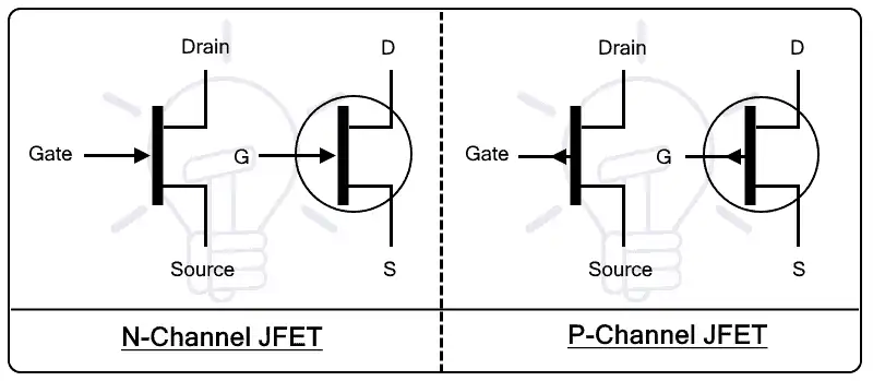
Selecting the right transistor depends on the specific application requirements. For low-power sensor interfaces, low-power transistors are ideal. They have limited heat output, high efficiency, and small size. This makes them suitable for compact packages and lightweight circuits. Efficiency and small size are prioritized over power handling in these applications. For ultra-low power sensor applications, engineers must select transistors with very low input thresholds. This allows operation at low voltages. Depletion mode N-channel Junction Field Effect Transistors (JFETs) are particularly suitable. They can operate at significantly lower thresholds (typically 20 mV to 100 mV gate-to-source pinch-off voltage) compared to silicon bipolar transistors (around 600 mV base-emitter voltage).
The choice between a BJT and a mosfet often comes down to a trade-off between cost, complexity, and performance.
|
Feature |
Bipolar Junction Transistor (BJT) |
MOSFET |
Implication for Sensor Interfaces |
|---|---|---|---|
|
Control Type |
Current-controlled (base current) |
Voltage-controlled (gate voltage) |
MOSFETs are easier to interface with logic outputs due to negligible gate current |
|
Input Impedance |
Moderate (kΩ range) |
Very high |
MOSFETs offer better noise immunity and easier interfacing |
|
Switching Speed |
Slower (due to storage time) |
High (minimal storage delay) |
MOSFETs excel in high-frequency switching applications |
|
Power Efficiency |
Higher saturation losses and heat |
Lower on-resistance and reduced heat |
MOSFETs provide better efficiency for low-loss switching |
|
On-State Voltage Drop |
Common Emitter Voltage (sat) ≈ 0.05–0.2 V |
Dependent on RDS(on); typically tens of milliohms |
MOSFETs can achieve lower conduction losses |
|
Cost and Complexity |
Typically cheaper; simple drive circuits |
Generally more expensive; sensitive to electrostatic discharge |
BJTs are often used for low-cost, low-frequency designs, while MOSFETs offer performance benefits at higher cost and complexity |
Engineers often choose BJTs for low-cost, low-frequency designs. MOSFETs offer performance benefits at a higher cost and complexity. The high-speed switching capability of a mosfet makes it a preferred choice for many modern power electronics.
In summary, BJTs are current-controlled devices, while a mosfet is voltage-controlled. These fundamental differences impact their operational characteristics and performance trade-offs. Neither transistor is universally superior; engineers select them based on specific circuit needs. For instance, BJTs excel in low-power amplification, while MOSFETs are ideal for high-power switching. Understanding these distinctions empowers designers to make informed choices for optimal circuit amplification, signal amplification, and overall performance of any transistor.
FAQ
What is the primary control difference between BJTs and MOSFETs?
BJTs are current-controlled devices. A small base current regulates a larger collector current. MOSFETs are voltage-controlled devices. A gate voltage creates an electric field that controls current flow between the source and drain.
Which transistor offers faster switching speeds?
MOSFETs generally offer faster switching speeds. Their voltage-controlled operation allows for rapid changes in state. BJTs have slower switching due to the time needed to manage stored charge carriers.
Do BJTs or MOSFETs have higher input impedance?
MOSFETs have a much higher input impedance. Their insulated gate draws almost no current. BJTs have a lower input impedance, requiring more current from the driving circuit.
Which transistor is more sensitive to electrostatic discharge (ESD)?
MOSFETs are generally more sensitive to ESD. Their gate insulation can easily break down from overvoltage. BJTs are less susceptible to ESD damage.
When should engineers choose a BJT instead of a MOSFET?
Engineers often choose BJTs for low-cost, low-frequency designs. They are good for audio amplification and current regulation. MOSFETs are preferred for high-speed switching and power efficiency.
See Also
USB Controller Comparison: Selecting CYUSB3014-BZXI or BZXC for Your Applications
IRF820 N-Channel MOSFET: Powering Management, DC-DC, and Motor Control
R5F64219JFB Microcontroller: Driving Audio Equipment Design with Core Performance
Coilcraft XPL2010: High-Performance Inductors for Advanced VRM/VRD Designs
MC9S12XEQ512CAL Microcontroller: Automotive to Industrial Control Deep-Dive Applications