Automotive engineers trust the OPA376AQDBVRQ1 to deliver reliable sensor performance in demanding environments. This operational amplifier supports accurate signal conditioning with its low input offset voltage and low noise design. Practical benefits include:
-
Reduced measurement errors for sensor signals
-
Enhanced signal integrity and power efficiency
-
Consistent operation across wide temperature ranges
-
Compliance with automotive-grade standards for robust performance
Its compact package fits easily into space-limited designs, making it a strong choice for modern sensor applications.
Key Takeaways
-
The OPA376AQDBVRQ1 offers high precision with very low offset voltage and low noise, ensuring accurate sensor readings in tough automotive environments.
-
Its automotive-grade design supports wide temperature ranges and meets strict quality standards, making it reliable for harsh conditions.
-
Proper circuit setup includes matching supply voltage, using the non-inverting configuration, and placing the amplifier close to the sensor to reduce noise.
-
Good PCB layout and grounding practices, along with filtering and shielding, help maintain clean signals and prevent interference.
-
Regular maintenance and careful component selection extend the sensor circuit’s life and keep performance stable over time.
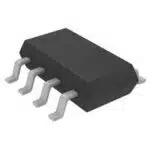
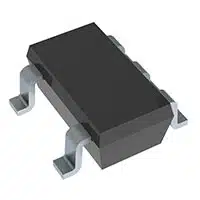
OPA376AQDBVRQ1 Features
Precision
Engineers rely on the OPA376AQDBVRQ1 for its outstanding precision in sensor signal conditioning. This operational amplifier uses advanced e-trim™ technology to achieve very low input offset voltage and minimal drift over temperature. These features help maintain accurate sensor readings, even in changing environments. The device also offers a rail-to-rail output, which allows the full use of the supply voltage range for better signal resolution.
The following table highlights key precision specifications:
|
Parameter |
Value/Range |
Description/Notes |
|---|---|---|
|
Input Offset Voltage (Vos) |
5 µV to 25 µV max |
Very low offset voltage supports precision |
|
Input Bias Current (Ib) |
0.2 pA to 10 pA |
Extremely low bias current for accuracy |
|
Common Mode Rejection Ratio |
76 dB to 90 dB |
High CMRR ensures noise rejection |
|
Input Offset Drift |
320 nV/K |
Low drift with temperature changes |
|
Gain Bandwidth Product |
5.5 MHz |
Frequency response characteristic |
|
Slew Rate |
2 V/µs |
Speed of output voltage change |
These specifications make the OPA376AQDBVRQ1 a strong choice for applications that demand high accuracy and stable performance.
Low Noise
Noise can distort sensor signals and reduce measurement accuracy. The OPA376AQDBVRQ1 addresses this challenge with a low noise density of 7.5 nV/√Hz. This low noise level helps preserve the integrity of small sensor signals, making it easier to detect subtle changes in the environment. The amplifier’s high common mode rejection ratio further reduces unwanted interference, supporting clean and reliable signal processing.
Designers can use the OPA376AQDBVRQ1 in circuits where low-level signals must be amplified without introducing extra noise. This feature is especially important in automotive and industrial sensor systems, where accuracy and reliability are critical.
Automotive Grade
The OPA376AQDBVRQ1 meets strict automotive standards, ensuring dependable operation in harsh conditions. The ‘Q1’ suffix in its name confirms that it is AEC-Q100 qualified. This qualification means the device has passed rigorous tests for reliability and quality, making it suitable for automotive applications.
Key automotive-grade features include:
-
Wide operating temperature range from -40°C to +125°C, supporting use in extreme environments.
-
Compact SOT-23-5 package, ideal for space-limited designs.
-
EMI hardening and e-trim™ technology for enhanced robustness and precision.
-
Designed for low noise, low offset voltage, and high accuracy in sensor signal conditioning.
-
Packaged for easy dispensing in automotive manufacturing processes.
These qualities make the OPA376AQDBVRQ1 a dependable solution for automotive sensor designs, where consistent performance and reliability are essential.
Integration Steps
Configuration
Engineers start by selecting the right configuration for the sensor circuit. The OPA376AQDBVRQ1 supports both single-supply and dual-supply operation. Most automotive sensor designs use a single-supply voltage between 2.2 V and 5.5 V. This range matches common automotive power rails. Designers choose the supply voltage based on the sensor type and system requirements.
Next, engineers set the amplifier in the correct mode. For most sensor applications, the non-inverting configuration works best. This setup allows the sensor signal to connect directly to the non-inverting input. The inverting input connects to a reference voltage, often ground or a mid-supply voltage. This approach ensures accurate amplification of the sensor signal.
Tip: Always review the sensor’s output range and match it with the amplifier’s input common-mode range. This step prevents signal clipping and distortion.
Connections
Proper connections ensure reliable signal transfer. Engineers connect the sensor output to the non-inverting input of the OPA376AQDBVRQ1. The inverting input connects to a reference voltage through a resistor network. This network sets the gain and helps balance the circuit.
Short and direct traces reduce noise pickup. Placing the amplifier close to the sensor minimizes interference. Engineers use shielded cables for long sensor leads. This practice protects the signal from electromagnetic interference (EMI).
A typical connection diagram looks like this:
Sensor Output ──► [Non-Inverting Input] OPA376AQDBVRQ1 [Output] ──► Signal Processing
                        │
                [Inverting Input] ──► Reference Voltage (Ground or Mid-Supply)
Note: Keep analog and digital grounds separate on the PCB. This separation reduces ground loops and noise.
Gain and Filtering
Setting the correct gain is important for accurate sensor readings. Engineers calculate the gain using external resistors. The gain formula for a non-inverting amplifier is:
Gain = 1 + (R2 / R1)
Where R1 connects from the inverting input to ground (or reference), and R2 connects from the inverting input to the output.
Engineers select resistor values that match the sensor’s output range to the input range of the next circuit stage. Using precision resistors improves accuracy.
Filtering removes unwanted noise from the sensor signal. Engineers add a capacitor in parallel with R2 to form a low-pass filter. This filter blocks high-frequency noise and ensures a clean signal.
Tip: Choose resistor and capacitor values that set the filter cutoff frequency just above the sensor’s maximum signal frequency.
Power and Ground
Stable power and proper grounding are key for reliable operation. Engineers use a clean, regulated supply voltage for the OPA376AQDBVRQ1. Placing a 0.1 µF ceramic capacitor close to the supply pin helps filter out high-frequency noise. Adding a larger capacitor, such as 1 µF, provides extra filtering for lower frequencies.
Ground connections should be short and direct. Engineers connect the amplifier’s ground pin to the analog ground plane. This practice reduces voltage drops and noise.
Alert: Avoid routing high-current traces near the amplifier. These traces can introduce noise and affect sensor accuracy.
Careful attention to power and ground layout ensures the amplifier delivers precise and stable sensor readings.
Reliability
Layout
Engineers achieve reliable sensor performance by following best practices in PCB layout. They place the amplifier close to the sensor to reduce noise and signal loss. Short, direct traces from the sensor to the amplifier input help maintain signal integrity. Wide traces for power and ground connections lower resistance and improve stability. A solid analog ground plane under the amplifier reduces voltage drops and shields sensitive signals from interference. Careful separation of analog and digital grounds prevents ground loops and unwanted noise.
Tip: Place decoupling capacitors as close as possible to the amplifier’s supply pins for best noise filtering.
EMI/EMC
Automotive environments often have strong electromagnetic interference. Engineers use several strategies to protect sensor circuits. Shielded cables and grounded enclosures block external noise. Ground planes and guard traces on the PCB help control electromagnetic fields. They route high-frequency or noisy signals away from sensitive analog paths. The device’s EMI-hardened design and high common-mode rejection ratio further reduce the impact of interference.
-
Use short, direct signal paths
-
Keep analog and digital circuits separate
-
Add ferrite beads or filters to power lines if needed
These steps help ensure clean, accurate sensor signals even in harsh environments.
Thermal
Automotive systems face wide temperature swings. The device operates reliably from -40°C to +125°C, making it suitable for engine compartments and other demanding locations. Its low offset voltage and minimal drift support stable measurements under thermal stress. The following table summarizes key thermal and electrical characteristics:
|
Parameter |
Value |
|---|---|
|
Operating Temperature Range |
-40°C to +125°C |
|
Maximum Operating Temp |
125°C |
|
Minimum Operating Temp |
-40°C |
|
Offset Voltage (max) |
25 µV |
|
Noise |
7.5 nV/√Hz |
|
Quiescent Current (max) |
950 µA |
|
Bandwidth |
5.5 MHz |
The device meets the AEC-Q100 automotive standard, which means it has passed rigorous reliability tests. This qualification, along with its robust design, ensures dependable operation in automotive and industrial environments.
Application Examples
Automotive engineers often use operational amplifiers to improve sensor accuracy and reliability. The OPA376AQDBVRQ1 supports a variety of sensor applications in vehicles. Below are three common examples that highlight its versatility.
Pressure Sensors
Pressure sensors monitor vital systems such as tire pressure, brake lines, and fuel rails. Engineers use the OPA376AQDBVRQ1 to amplify the small voltage changes from these sensors. Its low input offset voltage and low bias current help maintain accurate readings, even when signals are weak. A typical circuit places the amplifier close to the sensor, reducing noise and signal loss. The rail-to-rail output ensures the full sensor range reaches the vehicle’s control unit.
Tip: Place a low-pass filter at the amplifier output to remove high-frequency noise from the pressure signal.
Temperature Sensors
Temperature sensors protect engines and batteries by tracking heat levels. The OPA376AQDBVRQ1 excels in these circuits due to its precision and stability. Its low offset voltage and low noise density ensure accurate temperature readings, even in noisy environments. The amplifier’s wide operating temperature range matches the demands of automotive systems.
|
Parameter |
Value |
Benefit for Temperature Sensors |
|---|---|---|
|
Input Offset Voltage |
5 µV (max) |
High accuracy in signal conditioning |
|
Input Bias Current |
0.2 pA |
Minimal error in low-level signals |
|
Noise Density |
7.5 nV/√Hz |
Clean, precise temperature measurement |
|
Operating Temp Range |
-40°C to 125°C |
Reliable in harsh environments |
Engineers often use a simple voltage divider with a thermistor and connect the output to the amplifier’s non-inverting input. This setup delivers a stable, amplified signal to the vehicle’s monitoring system.
Current Sensing
Current sensing circuits help manage battery charging, motor control, and safety systems. The OPA376AQDBVRQ1 amplifies the voltage across a shunt resistor, providing accurate current measurements. Its high common mode rejection ratio ensures the signal remains clean, even near noisy power lines. The compact SOT-23-5 package fits easily into tight spaces, making it ideal for modern automotive modules.
Note: Use precision resistors for the shunt to maximize measurement accuracy.
Best Practices
Troubleshooting
Engineers sometimes face challenges when working with sensor circuits. Common issues include unexpected noise, signal drift, or inaccurate readings. To solve these problems, they should first check all connections. Loose wires or poor solder joints can cause signal loss. Engineers should also inspect the power supply. A noisy or unstable voltage source often leads to erratic amplifier behavior.
If the sensor output seems weak or distorted, engineers can measure the voltage at each amplifier pin. This step helps them find open circuits or incorrect biasing. Using an oscilloscope, they can look for unwanted high-frequency signals. Placing a small capacitor across the feedback resistor can help filter out this noise.
Tip: Replace suspect components with known good parts to rule out hardware faults.
A table below summarizes quick troubleshooting steps:
|
Problem |
Possible Cause |
Solution |
|---|---|---|
|
No output signal |
Open circuit |
Check wiring and solder joints |
|
Excessive noise |
Poor grounding |
Improve ground connections |
|
Signal drift |
Power supply issues |
Use stable, filtered supply |
|
Output clipping |
Gain set too high |
Adjust resistor values |
Long-Term Use
Long-term reliability matters in automotive sensor designs. Engineers should select high-quality resistors and capacitors with tight tolerances. These components help maintain accuracy over time. Regular inspection of solder joints and connectors prevents corrosion and mechanical wear.
Routine testing ensures continued performance. Engineers can use automated test equipment to check offset voltage, noise, and gain. Keeping the amplifier within its recommended temperature and voltage limits extends its lifespan. Cleaning the PCB removes dust and debris that might cause leakage currents.
Note: Document all maintenance and test results for future reference.
A checklist for long-term use includes:
-
Inspect and clean the PCB regularly
-
Verify supply voltage and ground integrity
-
Test amplifier parameters at scheduled intervals
-
Replace aging components as needed
Following these best practices helps engineers achieve reliable, long-lasting sensor circuits.
Engineers who use OPA376AQDBVRQ1 in automotive sensor designs gain reliable, precise, and robust performance. The device’s low offset voltage, low noise, and wide temperature range support accurate signal conditioning. The table below highlights important specifications:
|
Parameter |
Value |
|---|---|
|
Input Offset Voltage |
5 µV (typical) |
|
Input Noise |
7.5 nV/√Hz |
|
Supply Voltage Range |
2.2 V–5.5 V |
|
Operating Temp Range |
-40°C to +125°C |
|
Automotive Grade |
AEC-Q100 |
Engineers should follow best practices and review datasheets to ensure long-term success in their sensor designs.
What makes the OPA376AQDBVRQ1 suitable for automotive sensor designs?
The OPA376AQDBVRQ1 meets AEC-Q100 standards. It operates from -40°C to +125°C. Its low offset voltage and low noise help deliver accurate sensor readings. The compact SOT-23-5 package fits well in space-limited automotive modules.
Can engineers use the OPA376AQDBVRQ1 with both single and dual power supplies?
Yes. The OPA376AQDBVRQ1 works with single-supply voltages from 2.2 V to 5.5 V. It also supports dual-supply operation. This flexibility helps engineers match the amplifier to different automotive power systems.
How does the OPA376AQDBVRQ1 help reduce noise in sensor circuits?
The device features a low noise density of 7.5 nV/√Hz. Engineers can place the amplifier close to the sensor and use short traces. Adding a low-pass filter at the output further reduces unwanted high-frequency noise.
What are the key steps for reliable PCB layout with this amplifier?
Place the amplifier near the sensor.
Use short, direct traces for inputs and outputs.
Add decoupling capacitors close to the supply pins.
Keep analog and digital grounds separate to avoid noise.
Where can engineers find more technical details about the OPA376AQDBVRQ1?
Engineers can review the official Texas Instruments datasheet. The datasheet provides electrical characteristics, application notes, and layout guidelines. It helps ensure correct use in automotive sensor designs.
See Also
Simple Steps To Integrate Sensors Using SN74LVC4245APW
In-Depth Look At MC9S12DJ256MFUE For Automotive Use
How To Utilize ADXL357BEZ For Motion Sensing And Stability
Unveiling The Main Automotive Features Of FREESCALE MCF5251CVM140
Complete Overview Of AD1940YSTZ And AD1941YST Automotive DSPs